Pinouts
External Connectors
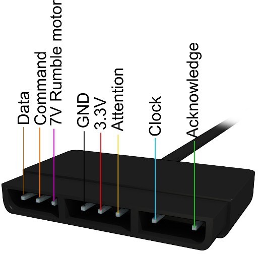
Pinouts - Controller Ports and Memory-Card Ports
Pinouts - Audio, Video, Power, Expansion Ports
Pinouts - SIO Pinouts
Internal Pinouts
Pinouts - Chipset Summary
Pinouts - CPU Pinouts
Pinouts - GPU Pinouts (for old 160-pin GPU)
Pinouts - GPU Pinouts (for new 208-pin GPU)
Pinouts - SPU Pinouts
Pinouts - DRV Pinouts
Pinouts - VCD Pinouts
Pinouts - HC05 Pinouts
Pinouts - MEM Pinouts
Pinouts - CLK Pinouts
Pinouts - PWR Pinouts
Pinouts - Component List and Chipset Pin-Outs for Digital Joypad, SCPH-1080
Pinouts - Component List and Chipset Pin-Outs for Analog Joypad, SCPH-1150
Pinouts - Component List and Chipset Pin-Outs for Analog Joypad, SCPH-1200
Pinouts - Component List and Chipset Pin-Outs for Analog Joypad, SCPH-110
Pinouts - Component List and Chipset Pin-Outs for Namco Lightgun, NPC-103
Pinouts - Component List and Chipset Pin-Outs for Multitap, SCPH-1070
Pinouts - Memory Cards
Mods/Upgrades
Mods - Nocash PSX-XBOO Upload
Mods - PAL/NTSC Color Mods
Pinouts - Controller Ports and Memory-Card Ports
Controller Ports and Memory-Card Ports
                   _______________________
Memory card slot: | 9 7 6 | 5 4 3 |  2 1  |
                  |_=_=_=_|_=_=_=_|__=_=__|
                   _______________________
                  | 9 8 7 | 6 5 4 | 3 2 1 |
Controller port:  | * * * | * * * | * * * |
                  '\______|_______|______/'
| Pin | Dir | Name | SIO0 pin | Description |
|---|---|---|---|---|
| 1 | In | DAT/MISO |
RX |
Serial data from device |
| 2 | Out | CMD/MOSI |
TX |
Serial data to device |
| 3 | +7.5V |
Supply for rumble motors | ||
| 4 | GND |
Ground | ||
| 5 | +3.5V |
Supply for main logic | ||
| 6 | Out | /CSn |
DTRn |
Port select |
| 7 | Out | SCK |
SCK |
Serial data clock |
| 8 | In | /IRQ |
/IRQ10 |
Lightgun IRQ (controller only) |
| 9 | In | /ACK |
DSR |
Data acknowledge IRQ |
/CSn are two separate signals (/CS1 for controller/memory card port 1, /CS2 for
port 2). All other signals are exactly the same on all four connectors (with the
memory card slots lacking the /IRQ pin and shield).
/IRQ pin
Most or all controllers leave pin 8 unused, the pin can be used as lightpen
input (not sure if the CPU is automatically latching a timer somewhere?), if
there's no auto-latched timer, then the interrupt would be required to be
handled as soon as possible; ie. don't disable interrupts, and don't "halt" the
CPU for longer periods (as far as I understood, the GTE can halt the CPU when
trying to read results of incomplete operations; to avoid that, one could wait
by software, eg. inserting NOPs, before reading GTE results...?)
(Some (or maybe all?) existing psx lightguns are reportedly connected to the
Video output on the Multiout port for determining the current cathode ray
position though).
Pinouts - Audio, Video, Power, Expansion Ports
AV Multi Out (Audio/Video Port)
  1      RGB-Video Green
  2      RGB-Video Red
  3      Supply +5.0V (eg. supply for external RF adaptor)
  4      RGB-Video Blue
  5      Supply Ground
  6      S-Video C (chrominance)
  7      Composite Video (yellow cinch)
  8      S-Video Y (luminance)                    ____________________________
  9      Audio Left      (white cinch)           |                            |
  10     Audio Left Ground                       | 12 11 10 9 8 7 6 5 4 3 2 1 |
  11     Audio Right     (red cinch)             |____________________________|
  12     Audio Right Ground
  Shield Video Ground
The plug on that cable does have additional sparings for pin 1,3,5 (though without any metal-contacts installed in there) (pin 3,5 would be used as supply for external RF modulators) (no idea what pin 1 could be used for though?).
RGB displays may (or may not) be able to extract /SYNC from the Composite signal, if that doesn't work, note that /SYNC (and separate /VSYNC, /HSYNC signals) are found on the GPU pinouts, moreover, the GPU outputs 24bit digital RGB.
Not sure if a VGA monitor can be connected? The SYNC signals are there (see GPU pinputs), but the vertical resolution is only 200/240 lines... standard VGA displays probably support only 400/480 lines (or higher resolutions for newer multisync SVGA displays) (as far as I know, the classic 200 lines VGA mode is actually outputting 400 lines, with each line repeated twice).
Parallel Port (PIO) (Expansion Port) (CN103)
This port exists only on older PSX boards (not on newer PSX boards, and not on
PSone boards).
The parallel port is used by various third-party unlicensed cheat cartridges and
VCD player addons, as well as by the PSIO optical drive emulator (see below).
             ________
            |        |                            Console Rear View
      GND ==| 1   35 |== GND                 .-------------------------.
   /RESET  =| 2   36 |=  DACK5               |1  2  3  ... ... 32 33 34|
    DREQ5  =| 3   37 |=  /IRQ10              |35 36 37 ... ... 66 67 68|
     /CS0  =| 4   38 |=  /WR1                |__.-------------------.__|
(SBEN)GND  =| 5   39 |=  GND(CS2)
       D0  =| 6   40 |=  D1
       D2  =| 7   41 |=  D3
       D4  =| 8   42 |=  D5
       D6  =| 9   43 |=  D7
       D8  =|10   44 |=  D9
      D10  =|11   45 |=  D11
      D12  =|12   46 |=  D13
      D14  =|13   47 |=  D15
       A0  =|14   48 |=  A1
       A2  =|15   49 |=  A3
      GND  =|16   50 |=  GND
    +3.5V ==|17   51 |== +3.5V
    +7.5V ==|18   52 |== +7.5V
      GND  =|19   53 |=  GND
       A4  =|20   54 |=  A5
       A6  =|21   55 |=  A7
       A8  =|22   56 |=  A9
      A10  =|23   57 |=  A11
      A12  =|24   58 |=  A13
      A14  =|25   59 |=  A15
      A16  =|26   60 |=  A17
      A18  =|27   61 |=  A19
      A20  =|28   62 |=  A21
      A22  =|29   63 |=  A23
      /RD  =|30   64 |=  /WR0
(/IRQ2)NC  =|31   65 |=  NC(/CS5)
    SYSCK  =|32   66 |=  LRCK
     BCLK  =|33   67 |=  SDIN
      GND ==|34   68 |== GND
            |________|
For more details see:
pcsx-redux - PIO port
pcsx-redux - Switch Board
Internal Power Supply (PSX)
The PSX contains an internal power supply, however, like the PSone, it's only
having a "Standby" button, which merely disconnects 3.5V and 7.9V from the
mainboard. The actual power supply remains powered, and wastes energy day and
night, thanks Sony!
External Power Supply (PSone)
  Inner +7.5V DC 2.0A   (inside diameter 0.8mm)
  Outer GND             (outside diameter 5.0mm)
Pinouts - SIO Pinouts
Serial Port
That port exists only on original Playstation (not on the PSone). The shape of
the Serial Port is identical to the 12pin Multiout (audio/video) port, but with
only 8pins.
  1 SIO1 In  RXD receive data    (from remote TXD)
  2 SIO2 -   VCC +3.5VDC         (supply, eg. for voltage conversion)
  3 SIO3 In  DSR                 (from remote DTR)           _________________
  4 SIO4 Out TXD transmit data   (to remote RXD)            |                 |
  5 SIO5 In  CTS clear to send   (from remote RTS)          | 8 7 6 5 4 3 2 1 |
  6 SIO6 Out DTR                 (to remote DSR)            |_________________|
  7 SIO7 -   GND Ground          (supply, eg. for voltage conversion)
  8 SIO8 Out RTS request to send (to remote CTS)
  Shield     GND Ground          (to/from remote GND)
PSone Serial Port
The PSone doesn't have an external serial connector, however, easy to use
soldering points for serial port signals are found as cluster of 5 soldering
points (below CPU pin52), and a single soldering point (below CPU pin100),
arranged like so (on PM-41 boards) (might be different on PM-41(2) boards):
                     CPU70.RTS
               CPU71.CTS   CPU74.TxD
                     CPU72.DTR   CPU75.RxD                       CPU73.DSR
If you want to upgrade the PSone, remove that resistors, and then install the PSX-style serial circuit (as shown below), or, think of a more simplified circuit without (dis-)inverted signals.
PSX Serial Port Connection (PU-23 board) (missing on PM-41 board)
The PSX serial circuit basically consists of a few transistors, diodes, and
resistors. The relevant part is that most of the signals are inverted -
compared with RS232 signals, the CPU uses normal high/low levels (of course
with 0V and 3.5V levels, not -12V and +12V), and the signals at the serial port
socket are inverted. Ie. if you want to built a RS232 adaptor, you must either
externally undo the inversion, or, disconnect the transistors, and wire your
circuit directly to the CPU signals.
  SIO8    SIO6    SIO4    SIO1    SIO3    SIO5    SIO2    SIO7---GND
    |       |       |       |       |       |      |
  FB112   FB114   FB116   FB115   FBnnn   FBnnn    o--L102-------3.5V
    |       |       |       |       |       |
    |       |       o-------|-------|-------|--------diode-------GND
    |       |       |       o-------|-------|--------diode-------GND
    |       |       |       |       o-------|--------diode-------GND
    |       |       |       |       |       o--------diode-------GND
    |       |       |       |       |       |
    |       |       |       o-------|-------|--------[1K]--------3.5V
    |       |       |       |       o-------|--------[1K]--------3.5V
   [22]    [22]    [22]    [22]     |       o--------[1K]--------3.5V
    |       |       |       |       |       |
   Q105-----|-------|-------|-------|-------|--------------------GND
    |      Q105-----|-------|-------|-------|--------------------GND
    |       |       |       |      Q106-----|--------------------GND
    |       |       |       |       |      Q106------------------GND
    |       |       |       |       |       |
    |       |       |       |       o-------|--------[470]-------3.5V
    |       |       |       |       |       o--------[470]-------3.5V
    |       |       |       |       |       |
   RTS     DTR     TxD     RxD     DSR     CTS
  CPU70   CPU72   CPU74   CPU75   CPU73   CPU71   <-- CPU Pin Numbers
   out     out     out     in      in      in
Note that there is no positive voltage protection (ie. +12V inputs would do no good, also strong -12V inputs might overheat the diodes/fuses, so if you want to use RS232 voltages, better use a circuit for voltage conversion).
Serial RS232 Adaptor
The PSX serial port uses 0V/3.5V logic, whilst RS232 uses -5V/+5V...-15V/+15V
logic. An example circuit for converting the logic levels would be:
    PSX.VCC--+||--PSX.GND  PSX.GND----DSUB.5.GND----DSUB.SHIELD  DSUB.1,9----NC
                   ______                                 ______
  ,-----------||+-|1   16|-------PSX.VCC ,-----------||+-|1   16|-------PSX.VCC
  | PSX.GND---||+-|2   15|-------PSX.GND | PSX.GND---||+-|2   15|-------PSX.GND
  '---------------|3   14|----DSUB.3.TXD '---------------|3   14|--- N/A
         ,---+||--|4   13|----DSUB.2.RXD        ,---+||--|4   13|--- N/A
         '--------|5   12|-------PSX.RXD        '--------|5   12|--- N/A
    PSX.GND--+||--|6   11|-------PSX.TXD   PSX.GND--+||--|6   11|--- N/A
    DSUB.7.RTS----|7   10|--o<|--PSX.RTS   DSUB.4.DTR----|7   10|--o<|--PSX.DTR
    DSUB.8.CTS----|8    9|--|>o--PSX.CTS   DSUB.6.DSR----|8    9|--|>o--PSX.DSR
                  |______|                               |______|
The four inverters are needed only for external adapters (which need to undo the transistor inversion on the PSX mainboard) (ie. the inverters are not needed when when connecting the circuit directly to the PSX CPU).
The second MAX232 chip is needed only if DTR/DSR "not ready" conditions are required (for an "always ready" condition: DSUB.4.DTR can be wired to -8.5V, which is available at Pin6 of the first MAX232 chip, and PSX.DSR can be wired to +3.5V).
With the above DSUB pin numbers, peripherals like mice or modems can be connected directly to the circuit. For connection to another computer, use a "null modem" cable (with crossed RXD/TXD, RTS/CTS, DTR/DSR wires).
The circuit works with both VCC=5V (default for MAX232) and with VCC=3.5V (resulting in slightly weaker signals, but still strong enough even for serial mice; which are mis-using the RS232 signals as power supply).
Pinouts - Chipset Summary
PSX/PSone Mainboards
  Board    Expl.
  PU-7     PSX, with AV multiout+cinch+svideo, GPU in two chips (160+64pins)
  PU-8     PSX, with AV multiout+cinch, four 8bit Main RAM chips
            EARLY-PU-8: "PU-8 1-658-467-11, N4" --> old chipset, resembles PU-7
            LATE-PU-8:  "PU-8 1-658-467-22, N6" --> new chipset, other as PU-7
  PU-9     PSX, without SCPH-number (just sticker saying "NOT FOR SALE, SONY)
  PU-16    PSX, with extra Video CD daughterboard (for SCPH-5903)
  PU-18    PSX, with AV multiout only, single 32bit Main RAM (instead 4x8bit)
  PU-20    PSX, unknown if/how it differs from PU-18
  PU-22    PSX, unknown if/how it differs from PU-18
  PU-23    PSX, with serial port, but without expansion port
  PM-41    PSone, older PSone, for GPU/SPU with RAM on-board (see revisions)
  PM-41(2) PSone, newer PSone, for GPU/SPU with RAM on-chip
  PM-41, 1-679-335-21  PSone with incomplete RGB signals on multiout port
  PM-41, 1-679-335-51  PSone with complete RGB signals on multiout port
The PM-41 board absorbed its external RAM across sub-revisions: -11..-51 use an external VRAM chip + external SPU-RAM chip (CXD8561 GPU + CXD2938Q SPU/CDROM); -61 switches to the CXD9500Q GPU with on-chip VRAM (but keeps the external SPU-RAM + CXD2938Q); only -71 ("PM-41(2)") adds the CXD2941R with on-chip SPU-RAM. So GPU-RAM was integrated one sub-revision before SPU-RAM.
CPU chips
  IC103 - 208pin - "SONY CXD8530BQ"  ;seen on PU-7 board
  IC103 - 208pin - "SONY CXD8530CQ"  ;seen on PU-7 and PU-8 boards
  IC103 - 208pin - "SONY CXD8606Q"   ;seen in PU-18 schematic
  IC103 - 208pin - "SONY CXD8606AQ"  ;seen on PU-xx? board
  IC103 - 208pin - "SONY CXD8606BQ"  ;seen on PM-41, PU-23, PU-20 boards
  IC103 - 208pin - "SONY CXD8606CQ"  ;seen on PM-41 board, too
GPU chips - Graphics Processing Unit
  IC203 - 160pin - "SONY CXD8514Q"   ;seen on PU-7 and EARLY-PU-8 boards
  IC203 - 208pin - "SONY CXD8561Q"   ;seen on LATE-PU-8 board
  IC203 - 208pin - "SONY CXD8561BQ"  ;seen on PU-18, PU-20 boards
  IC203 - 208pin - "SONY CXD8561CQ"  ;seen on PM-41 board
  IC203 - 208pin - "SONY CXD9500Q"   ;with on-chip RAM ;PM-41 -61 and PM-41(2) -71 boards
  IC21  - 208pin - "SONY CXD8538Q"   ;seen on GP-11 (namco System 11) boards
  IC103 - 208pin - "SONY CXD8654Q"   ;seen on GP-15 (namco System 12) boards
SPU chips - Sound Processing Unit
  IC308 - 100pin - "SONY CXD2922Q" (SPU)               ;PU-7 and EARLY-PU-8
  IC308 - 100pin - "SONY CXD2922BQ"(SPU)               ;EARLY-PU-8
  IC308 - 100pin - "SONY CXD2925Q" (SPU)               ;LATE-PU-8, PU-18, PU-20
  IC732 - 208pin - "SONY CXD2938Q" (SPU+CDROM)         ;PU-23 (PSX), PSone/PM-41 -11..-61
  IC732 - 176pin - "SONY CXD2941R" (SPU+CDROM+SPU_RAM) ;PSone/PM-41(2) (-71) Board
  IC402 - 24pin  - "AKM AK4309VM"  (Serial 2x16bit DAC);older boards only
  IC405 - 8pin   - "NJM2100E (TE2)" Audio Amplifier    ;PU-8 and PU-22 boards
  IC405 - 14pin  - "NJM2174" Audio Amplifier with Mute ;later boards
  IC405 - 14pin  - "NJM2790V (TE2)" Audio Amplifier    ;PM-41(2) (-71) board only
IC106 CPU-RAM / Main RAM chips
  IC106/IC107/IC108/IC109 - NEC 424805AL-A60 (28pin, 512Kx8) (PU-8 board)
  IC106 - "Samsung K4Q153212M-JC60" (70pin, 512Kx32) (newer boards)
  IC106 - "Toshiba T7X16 (70pin, 512Kx32) (newer boards, too)  ;PU-23 (SCPH-9000)
  IC106 - "Toshiba TC51V18325BJ-60S" (2MB) (PM-41 / PSone)
GPU-RAM / Video RAM chips
  IC201 - 64pin NEC uPD482445LGW-A70-S ;VRAM  ;\on PU-7 and EARLY-PU-8 board
  IC202 - 64pin NEC uPD482445LGW-A70-S ;VRAM  ;/split into 2 chips !
  IC201 - 64pin SEC KM4216Y256G-60     ;VRAM  ;\on other PU-7 board
  IC202 - 64pin SEC KM4216Y256G-60     ;VRAM  ;/split into 2 chips !
  IC201 - 100pin - Samsung KM4132G271BQ-10 (128Kx32x2)  ;-on later boards
  IC201 - 100pin - Samsung K4G163222A-PC70 (256Kx32x2)  ;-on PM-41
Note: The PM-41 board uses a 2MB VRAM chip (but allows to access only 1MB)
Note: The CXD9500Q GPU has on-chip RAM (no external VRAM); used from PM-41 -61 onwards (incl. PM-41(2) -71).
IC310 - SPU-RAM - Sound RAM chips
  IC310 - 40pin - "TOSHIBA TC51V4260DJ-70"  ;seen on PU-8 board
  IC310 - 40pin - EliteMT M11B416256A-35J (256K x 16bit)
  IC310 - "Fujitsu MB814260-70PJER" (256Kx16) ;PU-23, PM-41 (-11..-61)
  IC310 - "NN514267 ATT-50" (256Kx16)         ;PU-23 (PU23-11/-21/-31/-51)
BIOS ROM
  IC102 - 40pin - "SONY ..."          ;seen on PU-7 & early-PU-8 board (40pin!)
  IC102 - 44pin - "SONY M538032E-02"  ;seen on PU-16 (video CD, 1Mbyte BIOS)
  IC102 - 32pin - "SONY M534031C-25"  ;seen on later-PU-8 board
  IC102 - 32pin - "SONY 2022"         ;seen on PU-8 (1-658-467-23)
  IC102 - 32pin - "SONY 2030"         ;seen on PU-18 board
  IC102 - 32pin - "SONY M534031E-47"  ;seen on PM-41 board and PM-41(2)
  IC102 - 32pin - "SONY M27V401D-41"  ;seen on PM-41 board, too
  IC102 - 32pin - "OKI MSM534031E-07GS / -10GS" ;PU-23 (SCPH-9000)
  IC102 - 32pin - "Samsung KM23V4000DG-15"      ;PU-23 alternate source (SCPH-9000)
  IC102 - 32pin - "OKI MSM534031E-45/46/47GS"   ;PM-41 by model: 45=SCPH-100(JP), 46=101/103(US/Asia), 47=102(PAL)
Oscillators and Clock Multiplier/Divider
  X101 - 4pin - "67.737" (NTSC, presumably)         ;PU-7 .. PU-20
  X201 - 2pin - "17.734" (PAL) or "14.318" (NTSC)   ;PU-22 .. PM-41(2)
  IC204 - 8pin - "CY2081SL-500T" (NTSC) or "CY2081SL-509T" (PAL, marked "2294A") ;PU-22 .. PM-41(2)
Voltage Converter (for +7.5V to +5.0V conversion)
  IC601 - 3pin - "78M05" or "78005"  ;used in PSone
  IC601 - "Toshiba TA78M05F (TE16L)" (PU-23) or "MC78M05CDTRK" (PM-41) ;+5V regulator
Pulse-Width-Modulation Power-Control Chip
  IC606 16pin/10mm "TL594CD" (alternately to IC607) ;seen on PM-41 board
  IC607 16pin/5mm  "T594"    (alternately to IC606) ;seen on PM-41 board, too
  IC606/607/608 - PM-41 rev-dependent: "BA00AS" (-11), "TL594CD-R2" (-21), "TL594CPWR" (-31..-71), "MM1562FFBE" (-61/-71)
Reset Generator
  IC002 - 8pin - <not installed> (would be alternately to IC003) ;\on PSone
  IC003 - 5pin - <usually installed>                             ;/
  IC101 - 5pin - M51957B (Reset Generator) (on PSX-power supply boards)
  IC002/IC003 - "M51957BFP-600D" (reset/voltage detector) ;PM-41 (-11/-21)
  IC002/IC003 - "RN5VD13AA-TL"   (voltage detector)       ;PM-41 (-31..-71), replaces M51957B
CDROM Chips
  U42   80pin    SUB-CPU (CXP82300) with piggyback EPROM ;DTL-H2000
  IC304 80pin    SUB-CPU (MC68HC05L16) 80pin package     ;PU-7 and EARLY-PU-8
  IC304 52pin    SUB-CPU (MC68HC05G6) 52pin package      ;LATE-PU-8 and up
  IC305 - 100pin SONY CXD1199BQ (Decoder/FIFO)           ;PU-7
  IC305 - 100pin SONY CXD1815Q  (Decoder/FIFO)           ;PU-8, PU-18
  IC309 - 100pin SONY CXD2516Q  (Signal Processor)       ;PU-7 (100pin!)
  IC309 - 80pin  SONY CXD2510Q  (Signal Processor)       ;PU-8 and DTL-H2510
  IC702 - 48pin  SONY CXA1782BR (Servo Amplifier)        ;PU-7, PU-8
  IC101 - 100pin SONY CXD2515Q  (=CXD2510Q+CXA1782BR)    ;DTL-H2010
  IC701 - 100pin SONY CXD2545Q  (=CXD2510Q+CXA1782BR)    ;PU-18
  IC720 - 144pin SONY CXD1817R  (=CXD2545Q+CXD1815Q)     ;PU-20
  IC102 - 28pin - "BA6297AFP"           ;seen on DTL-H2010 drives
  IC704 - 28pin - "BA6398FP"            ;seen on PU-7
  IC722 - 28pin - "BA6397FP"            ;seen on late PU-8
  IC722 - 28pin - "BA5947FP"            ;seen on PM-41 and various boards
  IC722 - 28pin - "Panasonic AN8732SB"  ;seen on PM-41 board
  IC722 - 28pin - "Rohm BA5977FP-E2"    ;seen on PU-23 (SCPH-9000)
  IC722 - 28pin - "Rohm BA5947FP-E2"    ;seen on PM-41 (SCPH-100, confirms BA5947FP above)
  ICxxx - 20pin  SONY CXA1571N    (RF Amplifier) (on DTL-H2010 drives)
  IC703 - 20pin  SONY CXA1791N    (RF Amplifier) (on PU-18 boards)
  IC723 - 20pin  SONY CXA2575N-T4 (RF Matrix Amplifier) (on PU-22 .. PM-41(2))
Known IC304 (MC68HC05G6) mask-ROM part numbers by region (...2=JP/Asia, ...3=PAL, ...4=US):
  SC430942PB ;SCPH-9000/9003 (PU-23), SCPH-100/103 (PM-41 -11..-61)
  SC430943PB ;SCPH-9002 (PU-23, PAL), SCPH-102 (PM-41, PAL)
  SC430944PB ;SCPH-9001 (PU-23, US),  SCPH-101 (PM-41, US)
  SC430947PB ;SCPH-100/103 (PM-41(2) -71) ;new rev for CXD2941R
  SC430948PB ;SCPH-102     (PM-41(2) -71, PAL)
  SC430949PB ;SCPH-101     (PM-41(2) -71, US)
RGB Chips
  IC207 64pin "SONY CXD2923AR" VRAM Data to Analog RGB         ;\oldest
  IC501 24pin "SONY CXA1645M" Analog RGB to Composite          ;/
  IC202 44pin "Philips TDA8771H" Digital RGB to Analog RGB     ;\old boards
  IC202 44pin "Motorola MC141685FT" Digital RGB to Analog RGB  ;/
  IC?   48pin "H7240AKV" 24bit RGB to Analog+Composite         ;-SCPH-7001?
  IC502 48pin "SONY CXA2106R-T4" 24bit RGB to Analog+Composite ;-newer boards
MISC
  CDROM Drive: "KSM-440BAM" ;seen used with PM-41 board
  IC602 5pin "National LP2985IM5X-3.5" (3.5V LDO; top-marked "L/\1B" or "3DR") ;PU-23, PM-41 (-11..-61)
Controller/Memory Card Chips
  U?  24pin "9625H, CFS8121"     ;SCPH-1080, digital pad (alternate?)
  U?   ?pin "SC438001"           ;SCPH-1080, digital pad (alternate?)
  U?  32pin "(M), SC401800"      ;SCPH-1080, digital pad
  U?  32pin "(M), SC442116"      ;SCPH-xxxx, mouse
  IC? 64pin "SONY CXD103, -166Q" ;SCPH-1070, multitap
  U1  42pin "SD657, 9702K3006"   ;SCPH-1150, analog pad, single motor
  U1  42pin "SD657, 9726K3002"   ;SCPH-1180, analog pad, without motor
  U1  44pin "SONY CXD8771Q"      ;SCPH-1200, analog pad, two motors (PSX)
  U1  44pin "SD707, 039 107"     ;SCPH-110,  analog pad, two motors (PSone)
  U1  44pin "SD787A"             ;SCPH-xxx,  analog pad, two motors (PS2?)
  U?  64pin "SONY CXD8732AQ"     ;SCPH-1020, memory card, on-chip FLASH
  U?  XXpin other chips          ;SCPH-xxxx, memory card, external FLASH
  U1  44pin "NAMCO103P"          ;NPC-103, namco lightgun
Pinouts - CPU Pinouts
CPU Pinouts (IC103)
| Pin | Name | Pin | Name | Pin | Name | Pin | Name |
|---|---|---|---|---|---|---|---|
| 1 | VDD |
53 | VDD |
105 | VDD |
157 | VDD |
| 2 | VDD |
54 | VDD |
106 | VDD |
158 | VDD |
| 3 | CRYSTALN |
55 | RAM.A11 |
107 | SBUS.D0 |
159 | TIMER1.CLK |
| 4 | CRYSTALP |
56 | RAM.A10 |
108 | SBUS.D1 |
160 | TIMER0.CLK |
| 5 | RAM.D31 |
57 | RAM.A9 |
109 | SBUS.D2 |
161 | GPU.D0 |
| 6 | RAM.D30 |
58 | RAM.A8 |
110 | SBUS.D3 |
162 | GPU.D1 |
| 7 | RAM.D29 |
59 | RAM.A7 |
111 | SBUS.D4 |
163 | GPU.D2 |
| 8 | RAM.D28 |
60 | RAM.A6 |
112 | SBUS.D5 |
164 | GPU.D3 |
| 9 | RAM.D27 |
61 | RAM.A5 |
113 | SBUS.D6 |
165 | GPU.D4 |
| 10 | RAM.D26 |
62 | RAM.A4 |
114 | SBUS.D7 |
166 | GPU.D5 |
| 11 | RAM.D25 |
63 | RAM.A3 |
115 | SBUS.D8 |
167 | GPU.D6 |
| 12 | RAM.D24 |
64 | RAM.A2 |
116 | SBUS.D9 |
168 | GPU.D7 |
| 13 | RAM.D23 |
65 | GND |
117 | GND |
169 | GPU.D8 |
| 14 | VDD |
66 | VDD |
118 | VDD |
170 | GND |
| 15 | GND |
67 | RAM.A1 |
119 | SBUS.D10 |
171 | VDD |
| 16 | RAM.D22 |
68 | RAM.A0 |
120 | SBUS.D11 |
172 | GPU.D9 |
| 17 | RAM.D21 |
69 | /RC_NET |
121 | SBUS.D12 |
173 | GPU.D10 |
| 18 | RAM.D20 |
70 | SIO1./RTS |
122 | SBUS.D13 |
174 | GPU.D11 |
| 19 | RAM.D19 |
71 | SIO1./CTS |
123 | SBUS.D14 |
175 | GPU.D12 |
| 20 | RAM.D18 |
72 | SIO1./DTR |
124 | SBUS.D15 |
176 | GPU.D13 |
| 21 | RAM.D17 |
73 | SIO1./DSR |
125 | SBUS.A0 |
177 | GPU.D14 |
| 22 | RAM.D16 |
74 | SIO1.TX |
126 | SBUS.A1 |
178 | GPU.D15 |
| 23 | RAM.D15 |
75 | SIO1.RX |
127 | SBUS.A2 |
179 | GPU.D16 |
| 24 | RAM.D14 |
76 | /EXT_RESET |
128 | SBUS.A3 |
180 | GPU.D17 |
| 25 | RAM.D13 |
77 | SIO0./DTR2 |
129 | SBUS.A4 |
181 | GPU.D18 |
| 26 | VDD |
78 | GND |
130 | GND |
182 | GND |
| 27 | GND |
79 | VDD |
131 | VDD |
183 | VDD |
| 28 | RAM.D12 |
80 | SIO0./DTR1 |
132 | SBUS.A5 |
184 | GPU.D19 |
| 29 | RAM.D11 |
81 | SIO0./SCK |
133 | SBUS.A6 |
185 | GPU.D20 |
| 30 | RAM.D10 |
82 | SIO0./DSR |
134 | SBUS.A7 |
186 | GPU.D21 |
| 31 | RAM.D9 |
83 | SIO0.TX |
135 | SBUS.A8 |
187 | GPU.D22 |
| 32 | RAM.D8 |
84 | SIO0.RX |
136 | SBUS.A9 |
188 | GPU.D23 |
| 33 | RAM.D7 |
85 | SBUS.DACK5_PIO |
137 | SBUS.A10 |
189 | GPU.D24 |
| 34 | RAM.D6 |
86 | SBUS.DREQ5_PIO |
138 | SBUS.A11 |
190 | GPU.D25 |
| 35 | RAM.D5 |
87 | SBUS.DACK4_SPU |
139 | SBUS.A12 |
191 | GPU.D26 |
| 36 | RAM.D4 |
88 | SBUS.DREQ4_SPU |
140 | SBUS.A13 |
192 | GPU.D27 |
| 37 | RAM.D3 |
89 | /IRQ10_PIO |
141 | SBUS.A14 |
193 | GPU.D28 |
| 38 | VDD |
90 | /IRQ9_SPU |
142 | SBUS.A15 |
194 | GPU.D29 |
| 39 | GND |
91 | GND |
143 | GND |
195 | GND |
| 40 | RAM.D2 |
92 | VDD |
144 | VDD |
196 | VDD |
| 41 | RAM.D1 |
93 | /CSHTST |
145 | SBUS.A16 |
197 | GPU.D30 |
| 42 | RAM.D0 |
94 | /IRQ2_CDROM |
146 | SBUS.A17 |
198 | GPU.D31 |
| 43 | RAM./WE |
95 | SBUS./CS5_CDROM |
147 | SBUS.A18 |
199 | /IRQ0 |
| 44 | RAM./RAS1 |
96 | SBUS./CS4_SPU |
148 | SBUS.A19 |
200 | GPU.DREQ2 |
| 45 | RAM./RAS0 |
97 | SBUS./CS2_BIOS |
149 | SBUS.A20 |
201 | SYSCK0 |
| 46 | RAM./CAS3 |
98 | SBUS./CS0_EXP1 |
150 | SBUS.A21 |
202 | GPU.DACK2 |
| 47 | RAM./CAS2 |
99 | SBUS./WR1 |
151 | SBUS.A22 |
203 | GPU./WR |
| 48 | RAM./CAS1 |
100 | SBUS./WR0 |
152 | SBUS.A23 |
204 | GPU./RD |
| 49 | RAM./CAS0 |
101 | SBUS./RD |
153 | GPU.A0 |
205 | GPU./CS7 |
| 50 | VDD |
102 | /IRQ1_GPU |
154 | SYSCK1 |
206 | DSYSCK0 |
| 51 | GND |
103 | GND |
155 | GND |
207 | GND |
| 52 | GND |
104 | GND |
156 | GND |
208 | GND |
Pin5-68 = Main RAM bus. Pin 95-152 = System bus. Pin 102,153,159-206 = Video
bus.
CPU Pinout Notes
- On (some?) retail consoles,
RAM.A11is wired to the RAM chips' A8 line, whileRAM.A8andRAM.A10are left unconnected. RAM./RAS1is only used on systems with 4 or 8 MB RAM./RC_NETis tied to 3.5V, while/CSHTST(test pin?) is wired to ground.SYSCK0(33 MHz),DSYSCK0(67 MHz) andSYSCK1(33 MHz) are clock outputs from the CPU to the rest of the system.TIMER0.CLKis fed from the GPU'sDOTCKoutput, whileTIMER1.CLKis fed from itsHBLANKoutput.CRYSTALPandCRYSTALNare meant to be connected to a crystal, however all known console models feedCRYSTALPwith the clock generated by an external oscillator and leaveCRYSTALNopen.SBUS./WR1(upper byte write strobe) is routed to the expansion port but otherwise left unused, as all system bus devices are either 8-bit (CD-ROM, BIOS ROM) or only support 16-bit writes (SPU).SBUS.A0-SBUS.A23are latched outputs and are not affected by RAM and GPU addressing.
Pinouts - GPU Pinouts (for old 160-pin GPU)
Old 160-pin GPU is used on PU-7 boards and EARLY-PU-8 boards.
IC203 - Sony CXD8514Q - Old 160pin GPU for use with Dual-ported VRAM
Unlike the later 208pin GPU's, the old 160pin GPU has less supply pins, and, it
doesn't have a 24bit RGB output (nor any other video output at all), instead,
it's used with a RGB D/A converter that reads the video data directly from the
Dual-ported VRAM chips (ie. from special RAM chips with two data busses, one
bus for GPU read/write access, and one for the RGB video output).
  1-VCC     21-GND  41-D16  61-D2     81-D12'a  101-GND     121-D7'b 141-GND
  2-GND     22-D31  42-D15  62-D1     82-D11'a  102-DT/OE'b 122-D6'b 142-53MHz
  3-/GPUCS  23-D30  43-VCC  63-D0     83-D10'a  103-DT/OE'a 123-D5'b 143-VCC
  4-GPU.A2  24-D29  44-GND  64-GND    84-D9'a   104-/RAS    124-D4'b 144-GND
  5-/GPURD  25-D28  45-D14  65-VCC    85-D8'a   105-/WE'a   125-D3'b 145-FSC
  6-/GPUWR  26-D27  46-D13  66-A8'a   86-VCC    106-/WE'b   126-D2'b 146-VCC
  7-DACK2   27-D26  47-D12  67-A7'a   87-GND    107-/SE     127-D1'b 147-GND
  8-/RESET  28-VCC  48-D11  68-A6'a   88-D7'a   108-SC      128-D0'b 148-DOTCLK
  9-VCC     29-GND  49-D10  69-A5'a   89-D6'a   109-VCC     129-VCC  149-VCC
  10-GND    30-D25  50-GND  70-GND    90-D5'a   110-GND     130-GND  150-GND
  11-SYSCK0 31-D24  51-VCC  71-A4'a   91-D4'a   111-D15'b   131-A8'b 151-MEMCK1
  12-VCC    32-D23  52-D9   72-A3'a   92-D3'a   112-D14'b   132-A7'b 152-MEMCK2
  13-GND    33-D22  53-D8   73-A2'a   93-D2'a   113-D13'b   133-A6'b 153-BLANK
  14-DREQ2  34-D21  54-D7   74-A1'a   94-D1'a   114-D12'b   134-A5'b 154-/24BPP
  15-/IRQ1  35-D20  55-D6   75-A0'a   95-D0'a   115-D11'b   135-A4'b 155-/CSYNC
  16-HBLANK 36-VCC  56-D5   76-GND    96-VCC    116-D10'b   136-A3'b 156-/HSYNC
  17-VBLANK 37-GND  57-D4   77-VCC    97-DSF    117-D9'b    137-A2'b 157-/VSYNC
  18-high?  38-D19  58-D3   78-D15'a  98-/CAS'b 118-D8'b    138-A1'b 158-VCC
  19-high?  39-D18  59-GND  79-D14'a  99-/CAS'a 119-VCC     139-A0'b 159-GND
  20-VCC    40-D17  60-VCC  80-D13'a  100-VCC   120-GND     140-VCC  160-DSYSCK0
Pin 3,5,6,11,98,99,102,103,108,148,160 via 22 ohm. Pin 104,105,106 via 100 ohm. Pin 107 via 220 ohm. Pin 155 via 2200 ohm. Pin 145 via 220+2200 ohm.
  151-?       ---   (mem clock?)
  152-?             (mem clock?)
  153-BLANK         (high in HBLANK & VBLANK)
  154-/24BPP        (high=15bpp, low=24bpp)
  156-/HSYNC        rate:65us=15KHz, low:3.5us
  157-/VSYNC        rate:20ms=50Hz, low:130us=TwoLines
IC207 - SONY CXD2923AR - Digital VRAM to Analog RGB Converter (for old GPU)
This chip is used with the old 160pin GPU and two Dual-ported VRAM chips. The
2x16bit databus is capable of reading up to 32bits of VRAM data, and the chip
does then extract the 15bit or 24bit RGB values from that data (depending on
the GPU's current color depth).
The RGB outputs (pin 5,7,9) seem to be passed through transistors and
capacitors... not sure how the capacitors could output constant voltage
levels... unless the RGB signals are actually some kind of edge-triggering PWM
pulses rather than real analog levels(?)
  1-test?  9-BLUE    17-GND     25-D0'a  33-D8'a   41-D15'a  49-D7'b   57-D13'b
  2-test?  10-Vxx    18-MEMCK1  26-D1'a  34-D9'a   42-D0'b   50-D8'b   58-D14'b
  3-Vxx    11-test?  19-/24BPP  27-D2'a  35-D10'a  43-D1'b   51-D9'b   59-D15'b
  4-Vxx    12-test?  20-MEMCK2  28-D3'a  36-D11'a  44-D2'b   52-D10'b  60-GND
  5-RED    13-test?  21-BLANK   29-D4'a  37-D12'a  45-D3'b   53-D11'b  61-GND
  6-Vxx    14-aGND?  22-DOTCLK  30-D5'a  38-D13'a  46-D4'b   54-D12'b  62-GND
  7-GREEN  15-aGND?  23-GND     31-D6'a  39-D14'a  47-D5'b   55-GND    63-test?
  8-GND    16-aGND?  24-Vxx     32-D7'a  40-GND    48-D6'b   56-Vxx    64-GND
IC201 - 64pin NEC uPD482445LGW-A70-S or SEC KM4216Y256G-60 (VRAM 256Kx16)
IC202 - 64pin NEC uPD482445LGW-A70-S or SEC KM4216Y256G-60 (VRAM 256Kx16)
These are special Dual-ported VRAM chips (with two data busses), the D0-D15
pins are wired to the GPU (for read/write access), the Q0-Q15 pins are wired to
the RGB D/A converter (for sequential video output).
  1-VCC     9-Q2    17-D5    25-/UWE  33-GND   41-DSF  49-Q10   57-VCC
  2-/DT/OE  10-D2   18-VCC   26-/RAS  34-A3    42-GND  50-D11   58-D14
  3-GND     11-Q3   19-Q6    27-A8    35-A2    43-D8   51-Q11   59-Q14
  4-Q0      12-D3   20-D6    28-A7    36-A1    44-Q8   52-GND   60-D15
  5-D0      13-GND  21-Q7    29-A6    37-A0    45-D9   53-D12   61-Q15
  6-Q1      14-Q4   22-D7    30-A5    38-QSF   46-Q9   54-Q12   62-GND
  7-D1      15-D4   23-GND   31-A4    39-/CAS  47-VCC  55-D13   63-/SE
  8-VCC     16-Q5   24-/LWE  32-VCC   40-NC    48-D10  56-Q13   64-SC
IC501 24pin "SONY CXA1645M" Analog RGB to Composite (older boards only)
  1-GND1  4-BIN   7-NPIN   10-SYNCIN  13-IREF  16-YOUT   19-VCC2   22-GOUT
  2-RIN   5-NC    8-BFOUT  11-BC      14-VREF  17-YTRAP  20-CVOUT  23-ROUT
  3-GIN   6-SCIN  9-YCLPC  12-VCC1    15-COUT  18-FO     21-BOUT   24-GND2
Pin7 (NPIN): NTSC=VCC, PAL=GND. Pin6 (SCIN aka FSC): Sub Carrier aka PAL/NTSC color clock, which can be derived from three different sources:
  GPU pin 145 (old 160-pin GPU)
  GPU pin 154 (new 208-pin GPU)
  IC204 (on later boards, eg. PSone)
Pinouts - GPU Pinouts (for new 208-pin GPU)
New 206-pin GPU is used LATE-PU-8 boards and up.
GPU Pinouts (IC203)
| Pin | Name | Pin | Name | Pin | Name | Pin | Name |
|---|---|---|---|---|---|---|---|
| 1 | HOST./CS |
53 | HOST.D10 |
105 | GND |
157 | NTSC/PAL |
| 2 | HOST.A0 |
54 | HOST.D9 |
106 | VDD |
158 | /VSYNC |
| 3 | HOST./RD |
55 | HOST.D8 |
107 | SGRAM.D9 |
159 | /HSYNC |
| 4 | HOST./WR |
56 | HOST.D7 |
108 | SGRAM.D8 |
160 | DAC.B0 |
| 5 | HOST.DACK |
57 | HOST.D6 |
109 | SGRAM.D7 |
161 | DAC.B1 |
| 6 | /RESET |
58 | HOST.D5 |
110 | SGRAM.D6 |
162 | DAC.B2 |
| 7 | VDD |
59 | HOST.D4 |
111 | SGRAM.D5 |
163 | DAC.B3 |
| 8 | GND |
60 | GND |
112 | SGRAM.D4 |
164 | GND |
| 9 | /SYSCLK |
61 | VDD |
113 | GND |
165 | VDD |
| 10 | VDD |
62 | HOST.D3 |
114 | VDD |
166 | DAC.B4 |
| 11 | GND |
63 | HOST.D2 |
115 | SGRAM.D3 |
167 | DAC.B5 |
| 12 | HOST.DREQ |
64 | HOST.D1 |
116 | SGRAM.D2 |
168 | DAC.B6 |
| 13 | HOST./IRQ |
65 | HOST.D0 |
117 | SGRAM.D1 |
169 | DAC.B7 |
| 14 | HBLANK |
66 | GND |
118 | SGRAM.D0 |
170 | DAC.G0 |
| 15 | GND |
67 | VDD |
119 | GND |
171 | DAC.G1 |
| 16 | VDD |
68 | PCKSL2 |
120 | VDD |
172 | DAC.G2 |
| 17 | VBLANK |
69 | PCKSL1 |
121 | SGRAM./CS1 |
173 | DAC.G3 |
| 18 | HVHLD |
70 | PCKSL0 |
122 | SGRAM./CS0 |
174 | GND |
| 19 | GND |
71 | TEST3 |
123 | SGRAM.DSF |
175 | VDD |
| 20 | GND |
72 | TEST2 |
124 | SGRAM./RAS |
176 | DAC.G4 |
| 21 | NC |
73 | TEST1 |
125 | SGRAM./CAS |
177 | DAC.G5 |
| 22 | VDD |
74 | TEST0 |
126 | SGRAM./WE |
178 | DAC.G6 |
| 23 | VDD |
75 | VDD |
127 | SGRAM.DQMH |
179 | DAC.G7 |
| 24 | HOST.D31 |
76 | GND |
128 | SGRAM.DQML |
180 | DAC.R0 |
| 25 | HOST.D30 |
77 | SGRAM.D31 |
129 | GND |
181 | DAC.R1 |
| 26 | HOST.D29 |
78 | SGRAM.D30 |
130 | VDD |
182 | DAC.R2 |
| 27 | HOST.D28 |
79 | SGRAM.D29 |
131 | MCLKOUT |
183 | DAC.R3 |
| 28 | HOST.D27 |
80 | VDD |
132 | GND |
184 | GND |
| 29 | VDD |
81 | GND |
133 | VDD |
185 | VDD |
| 30 | GND |
82 | SGRAM.D28 |
134 | MCLKIN |
186 | DAC.R4 |
| 31 | HOST.D26 |
83 | SGRAM.D27 |
135 | GND |
187 | DAC.R5 |
| 32 | HOST.D25 |
84 | SGRAM.D26 |
136 | VDD |
188 | DAC.R6 |
| 33 | HOST.D24 |
85 | SGRAM.D25 |
137 | SGRAM.A9 |
189 | DAC.R7 |
| 34 | HOST.D23 |
86 | SGRAM.D24 |
138 | SGRAM.A8 |
190 | GND |
| 35 | HOST.D22 |
87 | VDD |
139 | SGRAM.A7 |
191 | VDD |
| 36 | HOST.D21 |
88 | GND |
140 | SGRAM.A6 |
192 | VCLK_NTSC |
| 37 | VDD |
89 | SGRAM.D23 |
141 | VDD |
193 | VDD |
| 38 | GND |
90 | SGRAM.D22 |
142 | GND |
194 | GND |
| 39 | HOST.D20 |
91 | SGRAM.D21 |
143 | SGRAM.A5 |
195 | VDD |
| 40 | HOST.D19 |
92 | SGRAM.D20 |
144 | SGRAM.A4 |
196 | VCLK_PAL |
| 41 | HOST.D18 |
93 | SGRAM.D19 |
145 | SGRAM.A3 |
197 | VDD |
| 42 | HOST.D17 |
94 | SGRAM.D18 |
146 | GND |
198 | GND |
| 43 | VDD |
95 | SGRAM.D17 |
147 | VDD |
199 | PCK |
| 44 | GND |
96 | GND |
148 | SGRAM.A2 |
200 | GND |
| 45 | HOST.D16 |
97 | VDD |
149 | SGRAM.A1 |
201 | VDD |
| 46 | HOST.D15 |
98 | SGRAM.D16 |
150 | SGRAM.A0 |
202 | DMASK |
| 47 | HOST.D14 |
99 | SGRAM.D15 |
151 | VDD |
203 | ODE2 |
| 48 | HOST.D13 |
100 | SGRAM.D14 |
152 | GND |
204 | GND |
| 49 | HOST.D12 |
101 | SGRAM.D13 |
153 | FSC |
205 | VDD |
| 50 | HOST.D11 |
102 | SGRAM.D12 |
154 | VDD |
206 | /DSYSCK |
| 51 | VDD |
103 | SGRAM.D11 |
155 | GND |
207 | GND |
| 52 | GND |
104 | SGRAM.D10 |
156 | CSYNC |
208 | VDD |
Pin 77..150 = Video RAM Bus. Pin 156..189 = Video Out Bus. Other = CPU Bus. Pin
153: Sub Carrier (NC on newer boards whick pick color clock from IC204).
GPU Pinout Notes
SGRAM./CS1is only used on arcade boards with 2 MB VRAM (two 1 MB chips).HVHLDis a lightgun input (similar to/IRQ10but handled in hardware) used only by some arcade boards. On retail consoles it has a 4.7k pullup to 3.5V.TEST0-TEST3are tied to 3.5V.PCKSL0-PCKSL2(outputs possibly related to the current horizontal/vertical resolution and thus pixel clock?) are left unconnected.MCLKINandMCLKOUTare tied together and wired to the DAC's clock input.MCLKINcould possibly be an external clock input for genlocking purposes.- On earlier motherboards and on most arcade boards only
VCLK_PALorVCLK_NTSCis wired up, depending on the console's region. On later boards both are tied together and connected to a programmable clock generator, which is preprogrammed to generate the appropriate frequency. /VSYNCand/HSYNCare only connected to test points./CSYNC = (/VSYNC AND /HSYNC).BLANK = (VBLANK OR HBLANK).SGRAM.DQMLis wired to bothDQM0andDQM2on the SGRAM, whileSGRAM.DQMHis wired to bothDQM1andDQM3.DMASKoutputs the mask/"alpha" bit of the current pixel and is used by some arcade boards to composite the GPU's output on top of an external video source.ODE2indicates which field is currently being output in interlaced mode.
IC202 44pin "Philips TDA8771H" Digital to Analog RGB (older boards only)
Region Japan+Europe: TDA8771AN
Region America+Asia: MC151854FLTEG or so?
  1-IREF  6-GNDd1  11-R1   16-G4   21-B7  26-B2     31-CLK    36-OUTB  41-NC
  2-GNDa1 7-VDDd1  12-R0   17-G3   22-B6  27-VDDd2  32-VDDa1  37-NC    42-GNDa2
  3-R7    8-R4     13-G7   18-G2   23-B5  28-GNDd2  33-VREF   38-NC    43-VDDa4
  4-R6    9-R3     14-G6   19-G1   24-B4  29-B1     34-NC     39-VDDa3 44-OUTR
  5-R5    10-R2    15-G5   20-G0   25-B3  30-B0     35-VDDa2  40-OUTG
Earlier boards are generating analog RGB via 64pin IC207, and later boards RGB via 48pin IC502.
IC502 48pin "SONY CXA2106R-T4" - 24bit RGB video D/A converter
| Pin | Name | Pin | Name | Pin | Name | Pin | Name |
|---|---|---|---|---|---|---|---|
| 1 | BCLAMP |
13 | NTSC/PAL |
25 | G7 |
37 | B3 |
| 2 | AGND2 |
14 | SYNCIN |
26 | G6 |
38 | B2 |
| 3 | ROUT |
15 | SCIN |
27 | G5 |
39 | B1 |
| 4 | GOUT |
16 | R7 |
28 | G4 |
40 | B0 |
| 5 | BOUT |
17 | R6 |
29 | G3 |
41 | VCLK |
| 6 | YOUT |
18 | R5 |
30 | G2 |
42 | DGND |
| 7 | COUT |
19 | R4 |
31 | G1 |
43 | VREFIN |
| 8 | VOUT |
20 | DVDD |
32 | G0 |
44 | VREFOUT |
| 9 | AVCC2 |
21 | R3 |
33 | B7 |
45 | AGND1 |
| 10 | YTRAP |
22 | R2 |
34 | B6 |
46 | RCRAMP |
| 11 | NC |
23 | R1 |
35 | B5 |
47 | AVCC1 |
| 12 | POWER_SAVE |
24 | R0 |
36 | B4 |
48 | GCLAMP |
Pin 3..8 (analogue outputs) are passed via external 75 ohm resistors.
Pin 6,7 additionally via 220uF. Pin 8 additionally via smaller capacitor.
Pin 10 (YTRAP) wired via 2K7 to 5.0V.
Pin 1,44,46,48 (can) connect via capacitors to ground (only installed for 44).
The 4.4MHz clock is obtained via 2K2 from IC204.Pin6.
The /PAL pin can be reportedly GROUNDED to force PAL colors in NTSC mode, when
doing that, you may first want to disconnect the pin from the GPU.
Note: Rohm BH7240AKV has same pinout (XXX but with pin7/pin8 swapped?)
Beware
Measuring in the region near GPU Pin10 is the nocash number one source for
blowing up components on the mainboard. If you want to measure that signals
while power is on, better measure them at the CPU side.
Pinouts - SPU Pinouts
IC308 - SONY CXD2922Q (SPU) (on PU-7, EARLY-PU-8 boards)
IC308 - SONY CXD2925Q (SPU) (on LATE-PU-8, PU-16, PU-18, PU-20 boards)
  1-D0    14-D11  27-A8    40-GND    53-3.5V  66-A15  79-5V    92-LRIA
  2-D1    15-GND  28-3.5V  41-SYSCK  54-GND   67-A14  80-A3    93-DTIA
  3-3.5V  16-D12  29-GND   42-GND    55-D7    68-A13  81-A2    94-BCIB
  4-GND   17-D13  30-A9    43-TEST   56-D6    69-A12  82-A1    95-LRIB
  5-D2    18-D14  31-/SPU  44-TES2   57-D5    70-A11  83-A0    96-DTIB
  6-D3    19-D15  32-/RD   45-D15    58-D4    71-A10  84-/WE0  97-BCKO
  7-D4    20-A1   33-/WR   46-D14    59-D3    72-A9   85-/OE0  98-LRCO
  8-D5    21-A2   34-DACK  47-D13    60-D2    73-A8   86-/WE1  99-DATO
  9-D6    22-A3   35-/IRQ  48-D12    61-D1    74-A7   87-/OE1  100-WCKO
  10-D7   23-A4   36-DREQ  49-D11    62-D0    75-A6   88-GND
  11-D8   24-A5   37-MUTE  50-D10    63-/RAS  76-A5   89-XCK
  12-D9   25-A6   38-/RST  51-D9     64-/CAS  77-A4   90-GND
  13-D10  26-A7   39-NC    52-D8     65-GND   78-GND  91-BCIA
IC732 - SONY CXD2941R (SPU+CDROM+SPU_RAM) (on PM-41(2) boards)
  1-DA16   23-FILO  45-LOCK  67-FSTO  89-SCSY   111-XCS   133-HD9   155-VSS5
  2-DA15   24-FILI  46-SSTP  68-COUT  90-SCLK   112-XRD   134-HD8   156-HA1
  3-DA14   25-PCO   47-SFDR  69-XDRST 91-SQSO   113-XWR   135-HD7   157-HA0
  4-VDDM0  26-CLTV  48-SRDR  70-DA11  92-SENS   114-HINT  136-HD6   158-VDDM3
  5-DA13   27-AVSSO 49-TFDR  71-DA10  93-DATA   115-XIRQ  137-VDD4  159-XCK
  6-DA12   28-RFAC  50-TRDR  72-DA09  94-XLAT   116-VDDM2 138-HD5   160-DTIB
  7-LRCK   29-BIAS  51-VSSM1 73-DA08  95-CLOK   117-XSCS  139-HD4   161-BCKO
  8-WDCK   30-ASYI  52-FFDA  74-AVSMO 96-XINT   118-XHCS  140-HD3   162-LRCO
  9-VDD0   31-AVDDO 53-FRDA  75-AVDMO 97-A4     119-XHRD  141-HD2   163-DAVDD0
  10-VSS0  32-ASYO  54-MDP   76-DA07  98-A3     120-XHWR  142-VSS4  164-DAREFL
  11-PSSL  33-VC    55-MDS   77-DA06  99-A2     121-DACK  143-HD1   165-AOUTL
  12-ASYE  34-CE    56-VDD2  78-VDDM1 100-A1    122-DREQ  144-HD0   166-DAVSS0
  13-GND   35-CEO   57-VSS2  79-DA05  101-A0    123-XRST  145-VSSM3 167-DAVSS1
  14-C4M   36-CEI   58-MIRR  80-DA04  102-D7    124-VDD3  146-HA9   168-AOUTR
  15-C16M  37-RFDC  59-DFCT  81-DA03  103-D6    125-SYSCK 147-HA8   169-DAREFR
  16-FSOF  38-ADIO  60-AVSM1 82-DA02  104-D5    126-VSS3  148-HA7   170-DAVDD1
  17-XTSL  39-AVDD1 61-AVDM1 83-DA01  105-D4    127-HD15  149-HA6   171-MUTO
  18-VDD1  40-IGEN  62-FOK   84-WFCK  106-VSSM2 128-HD14  150-HA5   172-DATO
  19-GND   41-AVSS1 63-PWMI  85-SCOR  107-D3    129-HD13  151-HA4   173-MTS3
  20-VPCO1 42-TE    64-FSW   86-SBSO  108-D2    130-HD12  152-VDD5  174-MTS2
  21-VPCO2 43-SE    65-MON   87-EXCK  109-D1    131-HD11  153-HA3   175-MTS1
  22-VCTL  44-FE    66-ATSK  88-SQCK  110-D0    132-HD10  154-HA2   176-MTS0
IC732 - SONY CXD2938Q (SPU+CDROM) (on newer boards) (PM-41 boards)
  1-SCLK    27-RFAC  53-TrckR 79-/XINT 105-A0    131-3.5V   157-(tst) 183-A8
  2-GNDed   28-GNDed 54-TrckF 80-SQCK  106-3.5V  132-D9     158-(tst) 184-A7
  3-GNDed   29-CLTV  55-FocuR 81-SQSO  107-A1    133-D8     159-GND   185-A6
  4-SBSO    30-PCO   56-3.5V  82-SENSE 108-A2    134-D7     160-D15   186-A5
  5-WFCK    31-FILI  57-FocuF 83-GND   109-A3    135-D6     161-D0    187-GND
  6-GNDed   32-FILO  58-SledR 84-GND   110-A4    136-D5     162-D14   188-A4
  7-C16M    33-VCTL  59-SledF 85-CD.D7 111-A5    137-3.5V   163-D1    189-A3
  8-3.5V    34-VPC02 60-NC    86-CD.D6 112-3.5V  138-D4     164-D13   190-A2
  9-C4M     35-VPC01 61-GND   87-CD.D5 113-A6    139-D3     165-3.5V  191-A1
  10-GNDed  36-VC    62-NC    88-CD.D4 114-A7    140-D2     166-D2    192-A0
  11-4.3MHz 37-FE    63-GND   89-CD.D3 115-A8    141-D1     167-D12   193-3.5V
  12-12MHz  38-SE    64-(tst) 90-CD.D2 116-A9    142-D0     168-D3    194-NC
  13-V16M   39-TE    65-(tst) 91-CD.D1 117-/IRQ2 143-GND    169-D11   195-(tst)
  14-DOUT   40-CE    66-note  92-CD.D0 118-/IRQ9 144-33MHzS 170-D10   196-GND
  15-LACK   41-CEO   67-note  93-3.5V  119-/RD   145-       171-D4    197-(tst)
  16-WDCK   42-CEI   68-(tst) 94-CD/CS 120-/WR   146-3.48V  172-D9    198-NC
  17-3.5Ved 43-RFDC  69-3.5V  95-CD/WR 121-DMA4  147-ZZ11   173-GND   199-NC
  18-LOCK   44-ADIO  70-(tst) 96-CD/RD 122-GND   148-GND    174-D5    200-NC
  19-GND    45-GND   71-(tst) 97-CD.A0 123-GND   149-GND    175-D8    201-3.5V
  20-MDS    46-IGEN  72-(tst) 98-CD.A1 124-/SPUW 150-ZZ7    176-D6    202-NC
  21-MDP    47-AVD1  73-(tst) 99-CD.A2 125-D15   151-3.48V  177-D7    203-NC
  22-3.5Ved 48-GNDed 74-DATA  100-GND  126-D14   152-/RES   178-/CAS  204-NC
  23-AVDO   49-GNDed 75-XLAT  101-CDA3 127-D13   153-3.5V   179-/WE   205-GND
  24-ASYO   50-GND   76-CLOK  102-CDA4 128-D12   154-ZZ5    180-3.5V  206-(tst)
  25-ASYI   51-GNDed 77-SCOR  103-/CD  129-D11   155-(tst)  181-/OE   207-(tst)
  26-BIAS   52-GNDed 78-GND   104-/SPU 130-D10   156-(tst)  182-/RAS  208-GND
Pin 21 and 53..59 = Drive Motor Control (IC722).
Pin 1..47 are probably mainly CDROM related.
Pin 39 "TE9" = IC723.Pin16 - CL709, and via 15K to SPU.39
Pin 66 connects via 4K7 to IC723.Pin19.
Pin 67 not connected (but there's room for an optional capacitor or resistor)
The (tst) pins are wired to test points (but not connected to any components)
CXD2938Q SPU Pinout Notes
Pin 74,75,76,119,120 are connected via 22 ohm.
Pin 103,104 are connected via 100 ohm.
ZZnn = IC405 Pin nn (analog audio related, L/R/MUTE).
Pin 103..142 = System Bus (BIOS,CPU). Pin 160..192 = Sound RAM Bus.
Pin 178 used for both /CASL and /CASH (which are shortcut with each other).
Pin 146 and 151 are 3.48V (another supply, not 3.5V).
Pin 147 and 150 are connected via capacitors.
Pin 195 and 197 testpoints are found below of the pin 206/207 testpoints.
 SPU155 (tst) always low         ;=maybe external audio (serial) this?
 SPU156 (tst) 45kHz  (22us)      ;=probably 44.1kHz (ext audio sample-rate)
 SPU157 (tst) 2777kHz  (0.36us)  ;=probably 64*44.1kHz (ext audio bit-rate)
 SPU158 (tst) always high        ;=maybe external audio (serial) or this?
SPU.Pin42 connects to ALL modchips
SPU.Pin42 via capacitor to SPU.Pin41, and via resistor?/diode? to IC723.10
CXD2938Q CDROM clocks
  SPU197  (*) 7.35kHz (44.1kHz/6) (stable clock, maybe DESIRED drive speed)
  SPU5    (*) 7.35kHz (44.1kHz/6) (unstable clock, maybe ACTUAL drive speed)
  SPU15   (*) 44.1kHz (44.1kHz*1)
  SPU16   (*) 88.2kHz (44.1kHz*2)
  SPU206  (*) circa 2.27MHz
  SPU70   (*) whatever clock (with SHORT low pulses)
CXD2938Q CDROM signals
  SPU207  fastsignal?
  SPU195  slowsignal?
  SPU18   usually high, low during seek or spinup or so
  SPU44   superslow hi/lo with superfast noise on it
  SPU73   mainly LOW with occasional HIGH levels...
  SPU71   LOW=SPIN_OK, PULSE=SPIN_UP/DOWN_OR_STOPPED
  SPU72   similar as SPU71
  SPU64   LOW=STOP, HI=SPIN
  SPU68   always low...?
  SPU65   whatever?
  SPU75   mainly HIGH, short LOW pulses when changing speed up/down/break
CXD2938Q CDROM/SPU Testpoints (on PM-41 board)
                |                                       | SPU73
                |          CXD2938Q (SPU)               |       SPU72
                |          (on PM-41 board)             | SPU70 SPU71
                |                                       | SPU64 SPU65 SPU68
  SPU206 SPU207 |_______________________________________|
   SPU197
    SPU195                   SPU16                   SPU44
                  SPU18 SPU5 SPU15
                          SPU12
IC402 - 24pin AKM AK4309VM (or AK4309AVM/AK4310VM) - Serial 2x16bit DAC
  1-TST?  4-/PD   7-CKS    10-LRCK  13-NC?    16-AOUTL  19-GNDa  22-VREFH
  2-VCCd  5-/RST  8-BICK   11-NC?   14-NC?    17-VCOM   20-NC?   23-VREFL
  3-GNDd  6-MCLK  9-SDATA  12-NC?   15-AOUTR  18-VCCa   21-NC?   24-DZF?
No 24pin AK4309VM datasheet exists (however it seems to be same as 20pin AK4309B's, with four extra NC pins at pin10-14).
IC405 - "2174, 1047C, JRC" or "3527, 0A68" (on newer boards)
Called "NJM2174" in service manual. Audio Amplifier with Mute.
  1  GND
  2  NC     ? via 100ohm to multiout pin 9    ;Audio Left (white cinch)
  3  OUT-R  ?
  4  MUTE1      ;specified as LOW = Mute
  5  MUTE2      ;specified as HIGH = Mute
  6  MUTEC      ;unspecified, maybe capacitor, or output based on MUTE1+MUTE2?
  7  IN-R     via capacitor to SPU.150
  8  BIAS
  9  NC
  10 NC
  11 IN-L     via capacitor to SPU.147
  12 OUT-L  ?
  13 NC     ? via 100ohm to multiout pin 11   ;Audio Right (red cinch)
  14 VCC      +5.0V (via L401)
IC405 - "NJM2100E (TE2)" Audio Amplifier (on older PU-8 and PU-22 boards)
  1-ROUT
  2-RIN- IC732.SPU.150
  3-RIN+
  4-GND
  5-LIN+
  6-LIN- IC732.SPU.147
  7-LOUT
  8-VCC 4.9V (+5.0V via L401)
Pinouts - DRV Pinouts
IC304 - 52pin/80pin - Motorola HC05 8bit CPU
IC305 - SONY CXD1815Q - CDROM Decoder/FIFO (used on PU-8, PU-16, PU-18)
  1-D0    14-/XINT 27-/HRD  40-GND   53-VDD   66-/MWR  79-GND   92-LRCO
  2-D1    15-GND   28-VDD   41-HDRQ  54-GND   67-MDB0  80-CLK   93-WCKO
  3-VDD   16-A0    29-GND   42-/HAC  55-MA8   68-MDB1  81-HCLK  94-BCKO
  4-GND   17-A1    30-/HWR  43-MA0   56-MA9   69-MDB2  82-CKSL  95-MUTE
  5-D2    18-A2    31-HD0   44-MA1   57-MA10  70-MDB3  83-RMCK  96-TD7
  6-D3    19-A3    32-HD1   45-MA2   58-MA11  71-MDB4  84-LRCK  97-TD6
  7-D4    20-A4    33-HD2   46-T01   59-MA12  72-MDB5  85-DATA  98-TD5
  8-D5    21-TD0   34-HD3   47-T02   60-MA13  73-MDB6  86-BCLK  99-TD4
  9-D6    22-/HRS  35-HD4   48-MA3   61-MA14  74-MDB7  87-C2PO  100-TD3
  10-D7   23-/HCS  36-HD5   49-MA4   62-MA15  75-MDBP  88-EMP
  11-/CS  24-HA0   37-HD6   50-MA5   63-MA16  76-XTL2  89-/RST
  12-/RD  25-HA1   38-HD7   51-MA6   64-/MOE  77-XTL1  90-GND
  13-/WR  26-HINT  39-HDP   52-MA7   65-GND   78-VDD   91-DATO
The pinouts/registers in CXD1199AQ datasheet are about 99% same as CXD1815Q.
Note: Parity on the 8bit data busses is NC. SRAM is 32Kx8 (A15+A16 are NC). Later boards have this integrated in the SPU.
ICsss - SONY CXA1782BR - CDROM Servo Amplifier (used on PU-8 boards)
  1-FEO    7-FE_M   13-RA_O  19-CLK    25-FOK   31-RF_O  37-FE_BIAS 43-LPFI
  2-FEI    8-SRCH   14-SL_P  20-XLT    26-CC2   32-RF_M  38-F       44-TEI
  3-FDFCT  9-TGU    15-SL_M  21-DATA   27-CC1   33-LD    39-E       45-ATSC
  4-FGD    10-TG2   16-SL_O  22-XRST   28-CB    34-PD    40-EI      46-TZC
  5-FLB    11-FSET  17-ISET  23-C.OUT  29-CP    35-PD1   41-GND     47-TDFCT
  6-FE_O   12-TA_M  18-VCC   24-SENS   30-RF_I  36-PD2   42-TEO     48-VC
IC309 - SONY CXD2510Q - CDROM Signal Processor (used on PU-8, PU-16 boards)
  1-FOK   11-PDO   21-GNDa 31-WDCK        41-DA09-XPLCK 51-APTL 61-EMPH 71-DATA
  2-FSW   12-GND   22-VLTV 32-LRCK        42-DA08-GFS   52-GND  62-WFCK 72-XLAT
  3-MON   13-TEST0 23-VDDa 33-VDD 5V      43-DA07-RFCK  53-XTAI 63-SCOR 73-VDD
  4-MDP   14-NC    24-RF   34-DA16-SDTA48 44-DA06-C2PO  54-XTAO 64-SBSO 74-CLOK
  5-MDS   15-NC    25-BIAS 35-DA15-SCLK48 45-DA05-XRAOF 55-XTSL 65-EXCK 75-SEIN
  6-LOCK  16-VPCO  26-ASYI 36-DA14-SDTA64 46-DA04-MNT3  56-FSTT 66-SQSO 76-CNIN
  7-NC    17-VCKI  27-ASYO 37-DA13-SCLK64 47-DA03-MNT2  57-FSOF 67-SQCK 77-DATO
  8-VCOO  18-FILO  28-ASYE 38-DA12-LRCK64 48-DA02-MNT1  58-C16M 68-MUTE 78-XLTO
  9-VCOI  19-FILI  29-NC   39-DA11-GTOP   49-DA01-MNT0  59-MD2  69-SENS 79-CLKO
  10-TEST 20-PCO   30-PSSL 40-DA10-XUGF   50-APTR       60-DOUT 70-XRST 80-MIRR
IC701 - SONY CXD2545Q - Signal Processor + Servo Amp (used on PU-18 boards)
  1-SRON  14-TEST 27-TE   40-VDDa        53-DA09-XPLCK 66-FSTI 79-MUTE 92-DFCT
  2-SRDR  15-GND  28-SE   41-VDD         54-DA08-GFS   67-FSTO 80-SENS 93-FOK
  3-SFON  16-TES2 29-FE   42-ASYE        55-DA07-RFCK  68-FSOF 81-XRST 94-FSW
  4-TFDR  17-TES3 30-VC   43-PSSL        56-DA06-C2PO  69-C16M 82-DIRC 95-MON
  5-TRON  18-PDO  31-FILO 44-WDCK        57-DA05-XRAOF 70-MD2  83-SCLK 96-MDP
  6-TRDR  19-VPCO 32-FILI 45-LRCK        58-DA04-MNT3  71-DOUT 84-DFSW 97-MDS
  7-TFON  20-VCKI 33-PCO  46-DA16-SDTA48 59-DA03-MNT2  72-EMPH 85-ATSK 98-LOCK
  8-FFDR  21-VDDa 34-CLTV 47-DA15-SCLK48 60-DA02-MNT1  73-WFCK 86-DATA 99-SSTP
  9-FRON  22-IGEN 35-GNDa 48-DA14-SDTA64 61-DA01-MNT0  74-SCOR 87-XLAT 100-SFDR
  10-FRDR 23-GNDa 36-RFAC 49-DA13-SCLK64 62-XTAI       75-SBSO 88-CLOK
  11-FFON 24-ADIO 37-BIAS 50-DA12-LRCK64 63-XTAO       76-EXCK 89-COUT
  12-VCOO 25-RFC  38-ASYI 51-DA11-GTOP   64-XTSL/GNDed 77-SQSO 90-VDD
  13-VCOI 26-RFDC 39-ASYO 52-DA10-XUGF   65-GND        78-SQCK 91-MIRR
IC101 - SONY CXD2515Q - Signal Processor + Servo Amp (used on DTL-H2010)
Pinouts are same as CXD2545Q, except, three pins are different: Pin24=ADII
(instead of ADIO), Pin25=ADIO (instead of RFC), Pin68=C4M (instead of FSOF).
IC720 - 144pin SONY CXD1817R (=CXD2545Q+CXD1815Q) ;PU-20
  1..48 - unknown
  49 - SCOR
  50..144 - unknown
IC701 - 8pin chip (on bottom side, but NOT installed) (PU-7 and EARLY-PU-8)
1-8 Unknown (maybe CDROM related, at least it's near other CDROM chips)
IC722 "BA5947FP" or "Panasonic AN8732SB" - IC for Compact Disc Players
Drive Motor related.
  1 to pin24,27
  2 SPINDLE            - via 15K to SPU21
  3 SW (ON/OFF)        - IC304.27
  4 TRACKING FORWARD
  5 TRACKING REVERSE
  6 FOCUS FORWARD
  7 FOCUS REVERSE
  8 GND                - CN702 pin 11
  9 NC (INTERNAL)      - via C731 (10uF) to GND
  10 +7.5V (Pow VCC ch1,2)
  11 FOCUS COIL (1)    - CN702 pin 15
  12 FOCUS COIL (2)    - CN702 pin 14
  13 TRACKING COIL (1) - CN702 pin 16
  14 TRACKING COIL (2) - CN702 pin 13
  15 SPINDLE MOTOR (1) - CN701 pin 4
  16 SPINDLE MOTOR (2) - CN701 pin 3
  17 SLED MOTOR (1)    - CN701 pin 1
  18 SLED MOTOR (2)    - CN701 pin 2
  19 +7.5V (Pow VCC ch3,4)
  20 MUTE              - /RES (via 5K6)
  21 GND
  22 SLED REVERSE
  23 SLED FORWARD
  24 to pin1
  25 via capacitors to pin1
  26 BIAS 1.75V
  27 to pin1
  28 +7.5V (Pre VCC)
IC703 - 20pin - "SONY CXA1791N" (RF Amplifier) (on PU-18 boards)
  1 LD       O APC amplifier output
  2 PD       I APC amplifier input
  3 PD1      I Input 1 for RF I-V amplifiers
  4 PD2      I Input 2 for RF I-V amplifiers
  5 GND/VEE  - Supply Ground
  6 F        I Input F for I-V amplifier
  7 E        I Input E for I-V amplifier
  8 VR       O DC Voltage Output (VCC+VEE)/2
  9 VC       I Center Voltage Input
  10 NC      - NC
  11 NC      - NC
  12 EO      O Monitoring Output for I-V amplifier E
  13 EI      - Gain Adjust for I-V amplifier E
  14 TE      O Tracking Error Amplifier Output
  15 FE_BIAS I BIAS Adjustment for Focus Error
  16 FE      O Focus Error Amplifier Output
  17 RFO     O RF Amplifier Output
  18 RFI     I RF Amplifier Input
  19 /LD_ON  I APC amplifier ON=GND, OFF=VCC
  20 VCC     - Supply
IC723 - 20pin - "SONY CXA2575N-T4" (RF (Matrix?) Amplifier) (PU-22..PM-41(2))
  1-TEIM
  2-TEIG
  3-VEE     GND
  4-E       via 33K to CN702 pin 4
  5-F       via 33K to CN702 pin 8
  6-PD2     via 36K to CN702 pin 6
  7-PD1     via 36K to CN702 pin 7
  8-PD      to CN702 pin 9
  9-LD
  10-VC     CL710, and CN702.Pin3, and via resistor?/diode? to SPU42
  11-LD_ON    IC304.Pin49 "LDON"  ..... XXX or is that Pin 20 "LD_ON" ?
  12-G_CONT                                                        ;or AL/TE?
  13-RF0    CL704, and...
  14-RFM
  15-FE     CL708, and...                 (maybe focus error?)
  16-TE     CL709, and via 15K to SPU.39  (maybe tracking error?)
  17-TE0
  18-COMP+
  19-MIRR   via 4K7 to SPU66
  20-VCC    3.48V (not 3.5V)
There is no CXA2575N datasheet (but maybe some signals do resemble CXA2570N/CXA2571N/CXA1791N datasheets).
CN702 CDROM Data Signal socket (PU-23 and PM-41 board)
  1-LD     to Q701
  2-VCC    to Q701
  3-VC     to IC723.Pin10 (and CL710)
  4-F-     to IC723.Pin4 (via 33K ohm)
  5-NC     to CL776
  6-PD2    to IC723.Pin6 (via 33K ohm)
  7-PD1    to IC723.Pin7 (via 33K ohm)
  8-E-     to IC723.Pin5 (via 33K ohm)
  9-M1     to IC723.Pin8
  10-VR    via 91 ohm to GND
  11-GND   GND
  12-LS    /POS0 (switch, GNDed when at head is at inner-most position)
  13-FCS+  TRACKING COIL (2)   ;\
  14-TRK+  FOCUS COIL (2)      ; or swapped?
  15-TRK   FOCUS COIL (1)      ;
  16-FCS   TRACKING COIL (1)   ;/
CN701 CDROM Motor socket (PU-8, PU-18, PU-23, PM-41 boards)
  1-SL-   SLED MOTOR (1)
  2-SL+   SLED MOTOR (2)
  3-SP+   SPINDLE MOTOR (2)
  4-SP-   SPINDLE MOTOR (1)
CLnnn - Calibration Points (PU-23 and PM-41 boards)
  CL616 +7.5V (PM-41 only, not PM-23) (before power switch)
  CL617 GND   (PM-41 only, not PM-23)
  CL316 to IC304 pin 21
  CL704 to IC723.Pin13
  CL706 GND
  CL708 to IC723.Pin15
  CL709 to IC723.Pin16
  CL710 to IC723.Pin10, and CN702.Pin3
  CL711 via 1K to IC723.Pin15
  CL776 to CN702.Pin5
Pinouts - VCD Pinouts
SCPH-5903 Video CD PlayStation
VCD Mainboard "PU-16, 1-655-191-11" Component List
The overall design is very close to LATE-PU-8 boards (1-658-467-2x). Changed
components are IC102/IC304 (different kernel and cdrom firmware),
C318/C325/C327 (height reduced capacitors for mounting the daughterboard above
of them). Plus some extra components: Three triple multiplexors (for switching
between PSX and VCD audio/video), and the daughterboard connector.
  IC102 44pin SONY, M538032E-02, JAPAN 6465401 (uncommonly big BIOS, 1Mx8)
  IC304 52pin C 4021 SC430924PB (HC05 sub-cpu, with extra Video CD command 1Fh)
  C318   2pin S5        ;\tantalum capacitors with lower height (instead
  C325   2pin CA7       ; of the electrolytic capacitors on PU-8 boards)
  C327   2pin CA7       ;/
  ICnnn 16pin 4053C (Triple multiplexor, for Audio LRCK,BCLK,DATA) (PCB top)
  ICnnn 16pin 4053C (Triple multiplexor, for Video FSC,CSYNC)      (PCB bottom)
  ICnnn 16pin 2283  (Triple multiplexor, for Video R,G,B)          (PCB bottom)
  CNnnn 30pin Connector to daughterboard                           (PCB top)
VCD Daughterboard "MP-45, 1-665-192-11" Component List
  IC102   3pin  TA78M05F voltage regulator (7.5V to 5V) (Toshiba)
  IC104 120pin  CXD1852AQ Video CD decoder (Sony)
  IC106  40pin  MB814260-70 (256Kx16 DRAM) (Fujitsu) ;see also: IC114
  IC107  20pin  6230FV 649 115 (OSD, similar to BU6257AFV-E2) (PCB back)
  IC109  14pin  Y2932 (TLC2932 PLL) (TI) (for RGB.DAC.CLK)
  IC110  44pin  TDA8771AH Triple Video DAC for RGB (Philips) (PCB back)
  IC111  64pin  CXP10224-603R 732A02E (MCU) (Sony)
  IC112  14pin  HCT32A (74HCT32 Quad OR gate) (TI) (PCB back) (for RGB.DAC.CLK)
  IC113   8pin  H74 7H (single D-type flip-flop; OSD clock divider) (PCB back)
  IC114  40pin  MB814260-70 (256Kx16 DRAM) (Fujitsu) ;see also: IC106
  CN101  30pin  Male Connector (to female 30pin socket on PU-16 mainboard)
  X103    2pin  45.00MHz (for VCD decoder chip)
  X104    4pin  12.000MHz (for MCU chip)
  X105    2pin  28.636MHz (for VCD decoder chip) (8*3.579545 NTSC clock)
VCD Daughterboard Connector
                               .--.---.
                         GND  / 1   2 | GND
    (CXD1815Q.86)    CD.BCLK |  3   4 | CD.LRCK    (CXD1815Q.84)
    (CXD1815Q.87)    CD.C2PO |  5   6 | CD.DATA    (CXD1815Q.85)
                         GND |  7   8 | CD.SQCK    (CXD2510Q.67) CXP.31
         (TDA.44) VIDEO.OUTR |  9  10 | CD.SQSO    (CXD2510Q.66) CXP.29
                         GND | 11  12 | SIO.OUT    (HC05.51.PORTF1 to CXP.47)
         (TDA.40) VIDEO.OUTG | 13  14 | SIO.IN     (HC05.50.PORTF0 from CXP.48)
                         GND | 15  16 | SIO.CLK    (HC05.52.PORTF2 to CXP.49)
         (TDA.36) VIDEO.OUTB | 17  18 | VIDEO.FSC  (CXD1852AQ.95)
                         GND | 19  20 | VIDEO.CSYNC(CXD1852AQ.96)
          (PSU.3)       3.5V | 21  22 | 3.5V       (PSU.3)
          (PSU.1)       7.5V | 23  24 | AUDIO.FSXI (CXD1852AQ.103 to VCD)
          (PSU.7)       /RES | 25  26 | AUDIO.DATA (CXD1852AQ.100)
  (CXD1852AQ.102) AUDIO.BCLK | 27  28 | AUDIO.LRCK (CXD1852AQ.101)
                         GND | 29  30 | GND
                             '--------'
IC104 "Sony CXD1852AQ" (MPEG-1 Decoder for Video CD) (120 pin)
   1-GND   16-HD7   31-GND   46-MD4   61-GND   76-G/Y3  91-GND       106-XTL2O
   2-XTL0O 17-MA3   32-MA7   47-MD11  62-/VOE  77-G/Y4  92-HSYNC     107-XTL2I
   3-XTL0I 18-MA4   33-MA8   48-MD3   63-R/Cr0 78-G/Y5  93-VSYNC     108-VDD
   4-VDD   19-MA2   34-/RAS  49-MD12  64-R/Cr1 79-G/Y6  94-FID/FHREF 109-C2PO
   5-HA2   20-MA5   35-/MWE  50-MD2   65-R/Cr2 80-G/Y7  95-CBLNK/FSC 110-LRCI
   6-HA3   21-MA1   36-/CAS2 51-MD13  66-R/Cr3 81-B/Cb0 96-CSYNC     111-DATI
   7-HD0   22-GND   37-/CAS0 52-MD1   67-R/Cr4 82-B/Cb1 97-/SGRST    112-BCKI
   8-HD1   23-MA6   38-MD7   53-MD14  68-R/Cr5 83-B/Cb2 98-CLK0O     113-DOIN
   9-HD2   24-MA0   39-MD8   54-MD0   69-R/Cr6 84-B/Cb3 99-DOUT      114-/HCS
  10-HD3   25-BC    40-MD6   55-MD15  70-R/Cr7 85-B/Cb4 100-DATO     115-/HDT
  11-HD4   26-TCKI  41-MD9   56-OSDEN 71-G/Y0  86-B/Cb5 101-LRCO     116-HRW
  12-HD5   27-TDI   42-MD5   57-OSDB  72-G/Y1  87-B/Cb6 102-BCKO     117-/HIRQ
  13-HD6   28-TENA1 43-MD10  58-OSDG  73-G/Y2  88-B/Cb7 103-FSXI     118-/RST
  14-VDD   29-TDO   44-VDD   59-OSDR  74-VDD   89-DCLK  104-VDD      119-HA0
  15-GND   30-VST   45-GND   60-VDD   75-GND   90-VDD   105-GND      120-HA1
IC107 "6230FV" (OSD chip, similar to BU6257AFV-E2) (20 pin)
   1-SIO.CLK   5-VDD      9-TEST  13-BLK2   17-OSDG
   2-SIO./CS   6-/CKOUT  10-GND   14-VC2    18-OSDB
   3-SIO.DTA   7-OSCOUT  11-BLK1  15-OSDEN  19-/VSYNC
   4-/RESET    8-OSCIN   12-VC1   16-OSDR   20-/HSYNC
No datasheet (but pinouts are same/similar as for BU6257AFV, documented in several service manuals for tape decks with vcd player: HCD-V5500, HCD-V8900/V8900AV, HCD-V909AV).
IC111 "Sony CXP10224-603R" (8bit SPC700 CPU) (64pin LQFP)
   1-PB5=TP    17-PD5=/HCS       33-AVREF=VDD             49-PG5/SCK1=HC05.PF2
   2-PB4=TP    18-PD4=TP         34-AVDD=VDD              50-PG4=/RST.OUT
   3-PB3=HA3   19-PD3=TP         35-PF7/AN7=TP            51-PG3/TO=TP
   4-PB2=HA2   20-PD2=TP         36-PF6/AN6=OSD.DTA       52-PA7=TP
   5-PB1=HA1   21-PD1=TP         37-PF5/AN5=OSD./CS       53-PA6=TP
   6-PB0=HA0   22-PD0=TP         38-PF4/AN4=OSD.CLK       54-PA5=TP
   7-PC7=HD7   23-MP/TEST=GND    39-PF3/AN3=GND           55-PA4=TP
   8-PC6=HD6   24-XTAL=12MHZ     40-PF2/AN2=GND           56-VPP=VDD
   9-PC5=HD5   25-EXTAL=12MHZ    41-PF1/AN1=GND           57-VDD=VDD
  10-PC4=HD4   26-VSS=GND        42-PF0/AN0=10KtoGND      58-VSS=GND
  11-PC3=HD3   27-/RST=/RES      43-PE3/PWM1=TP           59-PA3=TP
  12-PC2=HD2   28-/CS0=VDD       44-PE2/PWM0=TP           60-PA2=TP
  13-PC1=HD1   29-SI0=CD.SQSO    45-PE1/INT2/EC=/VSYNC    61-PA1=TP
  14-PC0=HD0   30-SO0=TP         46-PE0/INT0=/HIRQ        62-PA0=TP
  15-PD7=HRW   31-/SCK0=CD.SQCK  47-PG7/SI1/INT1=HC05.PF1 63-PB7=TP
  16-PD6=/HDT  32-AVSS=GND       48-PG6/SO1=HC05.PF0      64-PB6=TP
Pinouts are same as in CXP811P24 datasheet (which uses SPC700 instruction set; that instruction set is also used by SNES sound CPU).
IC109 "TLC2932" (PLL) (14pin)
  1-LOGIC_VDD=5V            5-FIN-B=HSYNC.PLL 9-PFD_INHIBIT=GND  13-BIAS
  2-SELECT=5V               6-PFD_OUT         10-VCO_INHIBIT=GND 14-VCO_VDD=5V
  3-VCO_OUT=RGB.DAC.CLK.PLL 7-LOGIC_GND=GND   11-VCO_GND=GND
  4-FIN-A=FID/FHREF.PLL     8-NC              12-VCO_IN
IC112 "74HCT32" (Quad OR gate) (14pin)
   1-FID/FHREF.MPEG  4-HSYNC.MPEG   8-(low)  11-RGB.DAC.CLK.TDA  7-GND
   2-FID/FHREF.MPEG  5-HSYNC.MPEG   9-GNDed  12-RGB.DAC.CLK.PLL  14-VCC/5V
   3-FID/FHREF.PLL   6-HSYNC.PLL   10-GNDed  13-RGB.DAC.CLK.PLL
IC113 "H74 7H" (single D-type flip-flop; OSD clock divider) (8 pin)
1-CLK 2-D 3-/Q 4-GND 5-Q 6-/RES 7-/SET 8-VCC
ICnnn "4053C" (Triple multiplexor, for Audio LRCK,BCLK,DATA) (16pin)
  1-IN2B=DATA.VCD   5-IN3A=LRCK.SPU    9-SEL3=LRCK.SEL   13-IN1B=BCLK.VCD
  2-IN2A=DATA.SPU   6-/OE=GNDed       10-SEL2=DATA.SEL   14-OUT1=BCLK.OUT
  3-IN3B=LRCK.VCD   7-VEE=GNDed       11-SEL1=BCLK.SEL   15-OUT2=DATA.OUT
  4-OUT3=LRCK.OUT   8-GND=GND         12-IN1A=BCLK.SPU   16-VDD=VDD/3.5V
ICnnn "4053C" (Triple multiplexor, for Video FSC,CSYNC) (16pin)
  1-IN2B=FSC.VCD    5-IN3A=CSYNC.PSX   9-SEL3=CSYNC.SEL  13-IN1B=GNDed
  2-IN2A=FSC.PSX    6-/OE=GNDed       10-SEL2=FSC.SEL    14-OUT1=NCed
  3-IN3B=CSYNC.VCD  7-VEE=GNDed       11-SEL1=DUMMY.SEL  15-OUT2=FSC.OUT
  4-OUT3=CSYNC.OUT  8-GND=GND         12-IN1A=GNDed      16-VDD=VCC/5V
ICnnn "NJM2283" (Triple multiplexor, for Video R,G,B) (16pin)
  1-IN1B=R.VCD      5-OUT2=G.OUT       9-IN3B=B.VCD      13-V=VCC/5V
  2-SEL1=R.SEL      6-OUT3=B.OUT      10-GND3=81ohm/GND  14-IN2B=G.VCD
  3-OUT1=R.OUT      7-SEL3=B.SEL      11-IN2A=G.PSX      15-GND1=GND
  4-GND2=GND        8-IN3A=B.PSX      12-SEL2=G.SEL      16-IN1A=R.PSX
Pinouts - HC05 Pinouts
Motorola HC05 chip versions for PSX cdrom control
  80pin "4246xx" - MC68HC05L16, on-chip ROM (DTL-H120x & old retail consoles)
  80pin "MC68HC705L16CFU" - MC68HC705L16, on-chip ROM (DTL-H100x, and PU-9)
  52pin "SC4309xx" - MC68HC05G6, on-chip ROM (newer retail consoles)
IC304 - "C 3060, SC430943PB, G63C 185" (PAL/PSone) - CDROM Controller
Called "MC68HC05G6PB" in service manual (=8bit CPU).
  1  NC     NC (TEST:DTR/out) (VCD:AVSEL/out)   ;-Port F           ;PortF.Bit3
  2  VDD    3.5V
  3  NC     NC          ;\                                   ;maybe PortE.Bit7?
  4  NC     NC          ; maybe MSBs of Port E               ;maybe PortE.Bit6?
  5  NC     NC          ;/                                   ;maybe PortE.Bit5?
  6  DECA4  SPU102      ;\                                         ;PortE.Bit4
  7  DECA3  SPU101      ; Port E [04h], aka Address/Index          ;PortE.Bit3
  8  DECA2  SPU99       ;                                          ;PortE.Bit2
  9  DECA1  SPU98       ;                                          ;PortE.Bit1
  10 DECA0  SPU97       ;/                                         ;PortE.Bit0
  11 VSS    GND
  12 NDLY   GND     reserved for factory test, should be wired to VDD, not GND?
  13 /RES   /RES (via 5K6)
  14 OSC1   4.3MHz (SPU11)(used as external clock for some modchips)(low volts)
  15 OSC2   NC
  16 F-BIAS         aka FOK=NC (in SCPH-5500)                      ;PortB.Bit0
  17 CG     NC      aka CG=CG (in SCPH-5500)     ;this IS portb.1! ;PortB.Bit1
  18 LMTSW  /POS0 (switch, GNDed when head at inner-most position) ;PortB.Bit2
  19 DOOR   SHELL_OPEN                                             ;PortB.Bit3
  20 TEST2  NC                                                     ;PortB.Bit4
  21 TEST1  to CL316                                               ;PortB.Bit5
  22 COUT               NC                                         ;PortB.Bit6
  23 SENSE  SPU82  ;CXD2510Q.69                                    ;PortB.Bit7
  24 SUBQ   SPU81  ;CXD2510Q.66                                    ;PortC.Bit0
  25 NC     NC     ;NC                                             ;PortC.Bit1
  26 SQCK   SPU80  ;CXD2510Q.67                                    ;PortC.Bit2
  27 SPEED  IC722.Pin3 (SW)                                        ;PortC.Bit3
  28 AL/TE         ;transisor aka MIRROR=..   (in SCPH-5500);ISN'T PortB.Bit1 !
  29 ROMSEL        ;NC        aka ROMSEL=SCLK (in SCPH-5500)       ;PortC.Bit5
  30 /XINT  SPU79  ;CXD1815Q.14                                    ;PortC.Bit6
  31 SCOR   SPU77  ;CXD2510Q.63                                    ;PortC.Bit7
  32 VDD    3.5V
  33 DECD0  CD.D0       ;\                                         ;PortA.Bit0
  34 DECD1  CD.D1       ;                                          ;PortA.Bit1
  35 DECD2  CD.D2       ;                                          ;PortA.Bit2
  36 DECD3  CD.D3       ; Port A [00h], aka Data                   ;PortA.Bit3
  37 DECD4  CD.D4       ;                                          ;PortA.Bit4
  38 DECD5  CD.D5       ;                                          ;PortA.Bit5
  39 VSS    GND         ;
  40 DECD6  CD.D6       ;                                          ;PortA.Bit6
  41 DECD7  CD.D7       ;/                                         ;PortA.Bit7
  42 NC     NC                                               ;maybe PortD.Bit0?
  43 DATA   SPU74 (via 22 ohm)                                     ;PortD.Bit1
  44 XLAT   SPU75 (via 22 ohm)                                     ;PortD.Bit2
  45 CLOK   SPU76 (via 22 ohm)                                     ;PortD.Bit3
  46 DECCS  SPU94                                                  ;PortD.Bit4
  47 DECWR  SPU95                                                  ;PortD.Bit5
  48 DECRD  SPU96                                                  ;PortD.Bit6
  49 LDON   IC723.Pin11                                            ;PortD.Bit7
  50 NC     NC (TEST:TX/out)  (VCD:SIO.IN/in)   ;\PortF (used by   ;PortF.Bit0
  51 NC     NC (TEST:RX/in)   (VCD:SIO.OUT/out) ; Motorola Testmode;PortF.Bit1
  52 NC     NC (TEST:RTS/out) (VCD:SIO.CLK/out) ;/and VCD version) ;PortF.Bit2
OSC input (internally HC05 is running at OSC/2, ie. around 2MHz):
  PU-8      4.0000MHz from separate 4.000MHz oscillator (X302)
  PU-16     4.0000MHz from separate 4.000MHz oscillator (X302)
  DTL-H2000 4.1900MHz from separate 4.1900MHz oscillator (SPC700, not HC05)
  PU-18     4.2336MHz from CXD2545Q.pin68 (Servo+Signal) (FSOF=16.9344MHz/4)
  PU-20     4.2xxxMHz from CXD1817R.pin?  (Servo+Signal+Decoder)
  PM-41     4.2xxxMHz from CXD2938Q.pin11 (Servo+Signal+Decoder+SPU)
HC05 - 80pin version (pinout from MC68HC05L16 datasheet)
  1 VDD
  2 FP28/PE6    ;\
  3 FP29/PE5    ;
  4 FP30/PE4    ;
  5 FP31/PE3    ; Port E LSBs
  6 FP32/PE2    ;
  7 FP33/PE1    ;
  8 FP34/PE0    ;/
  9 FP35/PD7    ;\
  10 FP36/PD6   ; Port D MSBs
  11 FP37/PD5   ;
  12 FP38/PD4   ;/
  13 VLCD3
  14 VLCD2
  15 VLCD1
  16 VSS
  17 NDLY
  18 XOSC1
  19 XOSC2
  20 /RESET
  ---
  21 OSC1
  22 OSC2
  23 PA0        ;\
  24 PA1        ;
  25 PA2        ;
  26 PA3        ; Port A
  27 PA4        ;
  28 PA5        ;
  29 PA6        ;
  30 PA7        ;/
  31 PB0/KWI0   ;\
  32 PB1/KWI1   ;
  33 PB2/KWI2   ;
  34 PB3/KWI3   ; Port B
  35 PB4/KWI4   ;
  36 PB5/KWI5   ;
  37 PB6/KWI6   ;
  38 PB7/KWI7   ;/
  39 PC0/SDI    ;\
  40 PC1/SDO    ;
  ---           ;
  41 PC2/SCK    ; Port C
  42 PC3/TCAP   ;
  43 PC4/EVI    ;
  44 PC5/EVO    ;
  45 PC6/IRQ2   ;
  46 PC7/IRQ1   ;/
  47 VDD
  48 BP3/PD3            ;\
  49 BP2/PD2            ; Port D LSBs
  50 BP1/PD1            ;
  51 BP0 (no "PD0")     ;/
  52 FP0
  53 FP1
  54 FP2
  55 FP3
  56 FP4
  57 FP5
  58 FP6
  59 FP7
  60 VSS
  ---
  61 FP8
  62 FP9
  63 FP10
  64 FP11
  65 FP12
  66 FP13
  67 FP14
  68 FP15
  69 FP16
  70 FP17
  71 FP18
  72 FP19
  73 FP20
  74 FP21
  75 FP22
  76 FP23
  77 FP24
  78 FP25
  79 FP26
  80 FP27/PE7   ;- Port E MSB
HC05 - 32pin/64pin Versions
Sony's Digital Joypad and Mouse contain 32pin CPUs, which are probably also
HC05's:
Pinouts - Component List and Chipset Pin-Outs for Digital Joypad, SCPH-1080
Moreover, some old memory cards contain a 64pin Motorola SC419510FU (probably
also a HC05) with separate Atmel AT29LV010A (128Kx8 FLASH).
Pinouts - MEM Pinouts
IC102 - BIOS ROM (32pin, 512Kx8, used on LATE-PU-8 boards, and newer boards)
  1-A19  5-A7  9-A3   13-D0   17-D3  21-D7   25-A11  29-A14
  2-A16  6-A6  10-A2  14-D1   18-D4  22-/CE  26-A9   30-A17     ;/CE=/BIOS
  3-A15  7-A5  11-A1  15-D2   19-D5  23-A10  27-A8   31-A18
  4-A12  8-A4  12-A0  16-GND  20-D6  24-/OE  28-A13  32-3.5V    ;/OE=/RD
Datasheet for (MS-)M534031E does exist.
IC102 - BIOS ROM (40pin, 512Kx8, used on PU-7 boards, and EARLY-PU-8 boards)
  1-A18  6-A4   11-GND   16-D9   21-VCC  26-D6      31-GND(/BYTE) 36-A13
  2-A8   7-A3   12-/OE   17-D2   22-D4   27-D14     32-A17        37-A12
  3-A7   8-A2   13-D0    18-D10  23-D12  28-D7      33-A16        38-A11
  4-A6   9-A1   14-D8    19-D3   24-D5   29-A0(D15) 34-A15        39-A10
  5-A5   10-/CS 15-D1    20-D11  25-D13  30-GND     35-A14        40-A9
Datasheet for MX23L4100 does exist.
IC102 - BIOS ROM (44pin, 1Mx8, used on P16-boards, ie. VCD console)
  1-NC  5-A7 9-A3   13-GND 17-D1  21-D3  25-D12 29-D14    33-/BYT 37-A14 41-A10
  2-A19 6-A6 10-A2  14-/OE 18-D9  22-D11 26-D5  30-D7     34-A17  38-A13 42-A9
  3-A18 7-A5 11-A1  15-D0  19-D2  23-VCC 27-D13 31-D15/A0 35-A16  39-A12 43-NC
  4-A8  8-A4 12-/CE 16-D8  20-D10 24-D4  28-D6  32-GND    36-A15  40-A11 44-NC
CPU-RAM (four 28pin chips) (older boards)
Unknown.
Note: The newer 70pin RAM comes up without external /REFRESH signal, but maybe
the 28pin RAMs required refresh (the CPU has some odd delays once and when).
IC106 - CPU-RAM (single 70pin chip, on newer boards)
"Samsung K4Q153212M-JC60" (70pin, 512Kx32) (newer boards)
"Toshiba T7X16" (70pin, 512Kx32) (newer boards, too)
  1-VCC   11-N.C   21-DQ15  31-A3   41-N.C   51-DQ17  61-DQ24
  2-DQ0   12-VCC   22-N.C   32-A4   42-N.C   52-DQ18  62-DQ25
  3-DQ1   13-DQ8   23-N.C!  33-A5   43-/OE   53-DQ19  63-DQ26
  4-DQ2   14-DQ9   24-N.C   34-A6   44-/W    54-VSS   64-DQ27
  5-DQ3   15-DQ10  25-N.C   35-VCC  45-/CAS3 55-DQ20  65-VSS
  6-VCC   16-DQ11  26-N.C   36-VSS  46-/CAS2 56-DQ21  66-DQ28
  7-DQ4   17-VCC   27-/RAS  37-A7   47-/CAS1 57-DQ22  67-DQ29
  8-DQ5   18-DQ12  28-A0    38-A8   48-/CAS0 58-DQ23  68-DQ30
  9-DQ6   19-DQ13  29-A1    39-A9   49-N.C   59-VSS   69-DQ31
  10-DQ7  20-DQ14  30-A2    40-N.C  50-DQ16  60-N.C   70-VSS
Datasheet for K4Q153212M-JC60 does exist (the chip supports 27ns Hyper Page mode access, which seems to be used for DMA).
IC106/IC107/IC108/IC109 - CPU-RAM (four 28pin chips, on PU-8, PU-18 boards)
SEC KM48V514BJ-6 (DRAM 512Kx8) (four pieces = 512Kx32 = 2Mbyte)
  1-VCC  5-DQ3   9-A9     13-A3     17-A5  21-NC    25-DQ5
  2-DQ0  6-NC    10-A0    14-VCC    18-A6  22-/OE   26-DQ6
  3-DQ1  7-/W    11-A1    15-GND    19-A7  23-/CAS  27-DQ7
  4-DQ2  8-/RAS  12-A2    16-A4     20-A8  24-DQ4   28-GND
IC310 - SPU-RAM (512Kbyte)
EliteMT M11B416256A-35J (256K x 16bit) (40pin SOJ, PM-41 boards)
Nippon Steel NN514256ALTT-50 (256K x 16bit) (40pin TSOP-II, PU-23 boards)
Toshiba TC51V4260DJ-70 (40pin, PU-8 board) (PseudoSRAM)
  1-5.0V  6-5.0V   11-NC   16-A0    21-VSS  26-A8    31-I/O8   36-I/O12
  2-I/O0  7-I/O4   12-NC   17-A1    22-A4   27-/OE   32-I/O9   37-I/O13
  3-I/O1  8-I/O5   13-/WE  18-A2    23-A5   28-/CASH 33-I/O10  38-I/O14
  4-I/O2  9-I/O6   14-/RAS 19-A3    24-A6   29-/CASL 34-I/O11  39-I/O15
  5-I/O3  10-I/O7  15-NC   20-5.0V  25-A7   30-NC    35-VSS    40-VSS
Note: The /CASL and /CASH pins are shortcut with each other on the mainboard, both wired to the /CAS pin of the SPU (ie. always accessing 16bit data at once).
Note: The TSOP-II package (18mm length, super-flat and with spacing between pin 10/11 and 30/31) is used on PU-23 boards. The pinouts and connections are identical for SOJ and TSOP-II.
Note: Nippon Steels NN514256-series is normally 256Kx4bit, nethertheless, for some bizarre reason, their 256Kx16bit chip is marked "NN514256ALTT"... maybe that happened accidently in the manufacturing process.
Note: The PM-41(2) board has on-chip RAM in the SPU (no external memory chip).
IC303 - CDROM Buffer (32Kbyte)
"HM62W256LFP-7T" (SRAM 32Kx8) (PCB bottom side) (PU-8)
"SONY CXK5V8257BTM" 32Kx8 SRAM (PU-18)
  1-A14  4-A6  7-A3  10-A0  13-D2   16-D4  19-D7   22-/OE  25-A8   28-VCC
  2-A12  5-A5  8-A2  11-D0  14-GND  17-D5  20-/CS  23-A11  26-A13
  3-A7   6-A4  9-A1  12-D1  15-D3   18-D6  21-A10  24-A9   27-/WE
IC201 - GPU-RAM (1MByte) (or 2MByte, of which, only 1MByte is used though)
Samsung KM4132G271BQ-10 (128K x 32bit x 2 Banks, Synchronous Graphic RAM) 1MB
Samsung K4G163222A-PC70 (256K x 32bit x 2 Banks, Synchronous Graphic RAM) 2MB
  1-DQ3   13-DQ19  25-/WE     37-N.C 49-A6    61-DQ9   73-VDDQ  85-VSS  97-DQ0
  2-VDDQ  14-VDDQ  26-/CAS    38-N.C 50-A7    62-VSSQ  74-DQ24  86-N.C  98-DQ1
  3-DQ4   15-VDD   27-/RAS    39-N.C 51-A8    63-DQ10  75-DQ25  87-N.C  99-VSSQ
  4-DQ5   16-VSS   28-/CS     40-N.C 52-N.C   64-DQ11  76-VSSQ  88-N.C  100-DQ2
  5-VSSQ  17-DQ20  29-A9(BA)  41-N.C 53-DSF   65-VDD   77-DQ26  89-N.C
  6-DQ6   18-DQ21  30-NC(GND) 42-N.C 54-CKE   66-VSS   78-DQ27  90-N.C
  7-DQ7   19-VSSQ  31-A0      43-N.C 55-CLK   67-VDDQ  79-VDDQ  91-N.C
  8-VDDQ  20-DQ22  32-A1      44-N.C 56-DQM1  68-DQ12  80-DQ28  92-N.C
  9-DQ16  21-DQ23  33-A2      45-N.C 57-DQM3  69-DQ13  81-DQ29  93-N.C
  10-DQ17 22-VDDQ  34-A3      46-VSS 58-NC    70-VSSQ  82-VSSQ  94-N.C
  11-VSSQ 23-DQM0  35-VDD     47-A4  59-VDDQ  71-DQ14  83-DQ30  95-N.C
  12-DQ18 24-DQM2  36-N.C     48-A5  60-DQ8   72-DQ15  84-DQ31  96-VDD
Note: The PM-41(2) board has on-chip RAM in the GPU (no external memory chip).
Pinouts - CLK Pinouts
The "should-be" CPU clock is 33.868800 Hz (ie. the 44100Hz CDROM/Audio clock,
multiplied by 300h). However, the different PSX/PSone boards are using
different oscillators, multipliers and dividers, which aren't exactly reaching
that "should-be" value. The PSone are using a single oscillator for producing
CPU/GPU clocks, and for producing the TV/color signal:
  For PAL,  Fsc=4.43361875MHz (5^6*283.75Hz+25Hz) --> 4*Fsc=17.734MHz
  For NTSC, Fsc=3.579545MHz   (4.5*455/572 MHz)   --> 4*Fsc=14.318MHz
PSone/PAL - IC204 8pin - "CY2081, SL-509" or "2294A, 1913"
Clock Multiplier/Divider
  1 53MHz          ;17.734MHz*3 = 53.202 MHz (?)
  2 GND
  3 X1 17.734MHz
  4 X2 17.734MHz
  5 67MHz          ;17.734MHz*3*2*7/11 = 67.711636 MHz (?)
  6 4.4Mhz         ;17.734MHz/4 = 4.4335MHz  (?)  ;via 2K2 to IC502.pin15
  7 3.5V
  8 3.5V
PSone/NTSC - IC204 8pin "CY2081 SL-500" (PSone, and PSX/PU-20 and up)
Unknown. Uses a 14.318MHz oscillator, so multiply/divide factors must be
somehow different.
   3*3*7*5/2/11 = 14.3181818
   3*3*7*7*100  = 44100
14.3181818 * 3*7*11*64 / (5*5*5*5*5) = 67.737600
14.3181818 * 2*2*13/11 ... or so?
PSX/PAL
PU-7 and PU-8 boards are using three separate oscillators:
  X101: 67.737MHz (div2 = CPU Clock = 33.8685MHz) (div600h = 44.1kHz audio)
  X201: 53.20MHz (GPU Clock) (div12 = PAL color clock)
  X302: 4.000MHz (for CDROM SUB CPU)
PSX/NTSC
PU-7 and PU-8 boards are using three separate oscillators:
  X101: 67.737MHz (div2 = CPU Clock = 33.8685MHz) (div600h = 44.1kHz audio)
  X201: 53.69MHz (GPU Clock) (div15 = NTSC color clock)
  X302: 4.000MHz (for CDROM SUB CPU)
Pinouts - PWR Pinouts
Voltage Summary
  +7.5V  Used to generate other voltages and CDROM/Joypad/MemoryCard/Expansion
  +5.0V  Used for Multiout, IC405, and IC502, and IC602
  +3.5V  Used for most ICs, and for Joypad/MemoryCard/Expansion
  +3.48V Used for SPU and CDROM
  GND    Ground, shared for all voltages
Fuses
There are a lot of SMD elements marked FBnnn, these are NOT fuses (at least
they don't seem to blow-up whatever you do). The actual fuses are marked PSnnn,
found near the power switch and near the power socket.
IC601 3pin +5.0V "78M05, RZ125, (ON)"
  1 +7.5V
  2 GND
  3 +5.0V   (used for Multiout, IC405, and IC502)
IC602 - Audio/CDROM Supply
Called "LP29851MX-3.5" in service manual.
  1 VIN    5.0V (in)
  2 GND    GND
  3 ON/OFF 5.0V (in)
  4 NOISE  ?
  5 VOUT   3.48V (out)
IC002/IC003 - Reset Generator (PM-41 board)
  IC002  IC003  Expl.
  2      2      connected to Q002 (reset input?)
  5      5      connected via capacitor to GND
  6      1      reset-output (IC002=wired to /RES, IC003: via Q004 to /RES)
  7      -      7.5V
  4      3      GND
  1,3,8  4      NC
Note: Either IC002 or IC003/Q004 can be installed on PM-41 boards. Most or all boards seem to contain IC003/Q004.
Note: PSX consoles have something similar on the Power Supply boards (IC101: M51957B).
IC606/IC607 - TL594CD - Pulse-Width-Modulation Power-Control Chip
  1 1IN+
  2 1IN-
  3 FEEDBACK
  4 DTC
  5 CT
  6 RT
  7 GND
  8 C1
  9  E1
  10 E2
  11 C2
  12 VCC
  13 OUTPUT CTRL
  14 REF
  15 2IN-
  16 2IN+
Q602
  x +7.5V
  y +3.5V
  z REG
CN602 - PU-8, PU-9 board Power Socket (to internal power supply board)
  1 Brown   7.5V (actually 7.69V)
  2 Red     GND  Ground
  3 Orange  3.5V (actually 3.48V)
  4 Yellow  GND  Ground
  5 White   STAND-BY (3.54V, always ON, even if power switch is off)
  6 Blue    GND  Ground
  7 Magenta /RES Reset input (from power-on logic and reset button)
CN602 - PU-18, PU-23 board Power Socket (to internal power supply board)
  1 Brown   7.5V (actually 7.92V or so) (ie. higher than in PSone)
  2 Red     GND  Ground
  3 Orange  3.5V (actually 3.53V or so) (ie. quite same as PSone)
  4 Yellow  GND  Ground
  5 White   /RES Reset input (from power-on logic and reset button)
CN102 - Controller/memory card daughter-board connector (PU-23 board)
  1 /IRQ10 (/IRQ10)
  2 /ACK (/IRQ7)
  3 /JOY2
  4 7.5V (or actually 7.92V)
  5 /JOY1
  6 DAT
  7 GND
  8 CMD
  9 3.5V
  10 CLK
Pinouts - Component List and Chipset Pin-Outs for Digital Joypad, SCPH-1080
Digital Joypad Component List (SCPH-1080)
  Case: "SONY, CONTROLLER, Sony Computer Entertainment Inc. H"
  Case: "SCPH-1080 Made in China"
  PCB: "CMK-PIHB /\, CFS8121-200010-01"
  U?: 32pin "(M), SC401800, FB C37B, JSJD520C" (Motorola) (TQFP-32 package)
  U?: 14pin "BA10339F, 528 293" (Quad Comparator) (/ACK,JOYDAT,and reset or so)
  X?:  3pin "4.00G1f" (on PCB bottom side)
  Z1:  2pin z-diode or so (on PCB bottom side) (+1.7V VREF for BA10339F)
  CN?: 7pin cable to controller port (plus shield; but not connected to PCB)
  C1   2pin   to GND and R5
  C2   2pin capacitor for power supply input (between +3.5V and GND)
  C3   2pin   between BA.pin8 and (via R6) BA.pin15
  R1   2pin 1M ohm (for X1)
  R2   2pin 2.7K
  R3   2pin 8xK ohm?
  R4   2pin 100K
  R5   2pin 22K ohm
  R6   2pin 56K ohm
  RN1  8pin 4x200 ohm (/JOYn,JOYCMD,JOYCLK)
  RN2  8pin 4x22K ohm (pull-ups for button bit0..3)
  RN3  8pin 4x22K ohm (pull-ups for button bit12..15)
  RN4  8pin 4x22K ohm (pull-ups for button bit8..11)
  RN5  8pin 4x22K ohm (pull-ups for button bit4..7)
Digital Joypad Connection Cable:
  PSX.1 -------brown---- PAD.2 JOYDAT
  PSX.2 -------orange--- PAD.6 JOYCMD
  PSX.3 ---              NC    +7.5V
  PSX.4 -------black---- PAD.3 GND
  PSX.5 -------red------ PAD.4 +3.5V
  PSX.6 -------yellow--- PAD.5 /JOYn
  PSX.7 -------blue----- PAD.7 JOYCLK
  PSX.8 ---              NC    /IRQ10
  PSX.9 -------green---- PAD.1 /ACK
  PSX.Shield --shield--- NC    (cable is shielded but isn't connected in joypad)
Digital Joypad 32pin SC401800 Chip Pin-Outs
  1 Bit14 SW-X
  2 Bit13 SW-O
  3 Bit12 SW-/\
  4 Bit11 SW-R1 (via cable pin1, white wire)
  5 Bit10 SW-L1 (via cable pin1, white wire)
  6 Bit9  SW-R2 (via cable pin3, black wire)
  7 Bit8  SW-L2 (via cable pin3, black wire)
  8 via BA10339F.pin7 to cn.2 JOYDAT (PSX.1)
  ---
  9  via RN1 (200 ohm) to cn.5 /JOYn  (PSX.6)
  10 via RN1 (200 ohm) to cn.6 JOYCMD (PSX.2)
  11 via RN1 (200 ohm) to cn.7 JOYCLK (PSX.7)
  12 GND to cn.3 (PSX.4)
  13 Bit7 SW-LEFT
  14 Bit6 SW-DOWN
  15 Bit5 SW-RIGHT
  16 via BA10339F.pin5 to cn.1 /ACK (PSX.9)
  ---
  17 Bit4 SW-UP
  18 Bit3 SW-START
  19 Bit2 (HI) (would be R3 on Analog Pads) ;\unused, but working button inputs
  20 Bit1 (HI) (would be L3 on Analog Pads) ;/(each fitted with a RN2 pullup)
  21 Bit0 SW-SELECT
  22
  23
  24 wired to SC401800.pin25
  ---
  25 wired to SC401800.pin24
  26 4.00MHz'a
  27 4.00MHz'b
  28 +3.5V to cn.4 (PSX.5)
  29 wired to SC401800.pin32, and via 22K ohm to +3.5V, and to BA.14
  30
  31 Bit15 SW-[]
  32 wired to SC401800.pin29
Digital Joypad 14pin BA10339F Chip Pin-Outs
  1 OUT2  CN.2 JOYDAT (PSX.1)
  2 OUT1  CN.1 /ACK (PSX.9)
  3 VCC   +3.5V
  4 -IN1  +1.7V VREF via Z1 to GND
  5 +IN1  CXD.16 /ACK
  6 -IN2  +1.7V VREF via Z1 to GND
  7 +IN2  CXD.8  JOYDAT
  ---
  8 -IN3  +1.7V VREF via Z1 to GND
  9 +IN3      C3,R3,R4
  10 -IN4     C1 to +3.5V
  11 +IN4 GND
  12 GND  GND
  13 OUT4     NC ??
  14 OUT3 CXD.29/32
Pinouts - Component List and Chipset Pin-Outs for Analog Joypad, SCPH-1150
This applies for two controller versions:
  SCPH-1150 Analog Pad with Single Rumble Motor (japan only)
  SCPH-1180 Analog Pad without Rumble Motor
Analog Joypad Component List (SCPH-1150, single motor)
  Case "SONY, ANALOG, CONTROLLER, SonyCompEntInc. A, SCPH-1150 MADE IN CHINA"
  PCB1 "DD1P09A" (mainboard with digital buttons)
  PCB2 "DD1Q14A" (daughterboard with analog joysticks)
  PCB3 "DD1Q15A-R" (daughterboard with R-1, R-2 buttons) (J3)
  PCB4 "DD1Q15A-L" (daughterboard with L-1, L-2 buttons) (J2)
  U1  42pin "SD657, 9702K3006"   (2x21pins, L=17.8mm, W=7mm, W+Pins=11mm)
  U2   3pin "DR, 4.Z"
  Q1   3pin "BQ03" or so (motor post-amp)
  Q2   3pin "S6","SG","9S" or so (motor pre-amp)
  Y1   3pin "400CMA"
  CN1  8pin cable to PSX controller port
  CN2  8pin ribbon cable to analog-joystick daughterboard (not so robust cable)
  J1   2pin wires to rumble motor (in left handle) (digital, on/off)
  J2   3pin ribbon cable to L-1, L-2 button daughterboard
  J3   3pin ribbon cable to R-1, R-2 button daughterboard
  LED1 4pin red/green LED (optics without mirror)
  D1,D2 diodes
  plus resistors/capacitors
Analog Joypad Connection Cables (SCPH-1150)
CN1 (cable to PSX controller port) (same for SCPH-1150 and SCPH-1200)
  PSX.1 -------brown---- PAD.2 JOYDAT
  PSX.2 -------orange--- PAD.6 JOYCMD
  PSX.3 -------magenta-- PAD.8 +7.5V
  PSX.4 -------black---- PAD.3 GND
  PSX.5 -------red------ PAD.4 +3.5V
  PSX.6 -------yellow--- PAD.5 /JOYn
  PSX.7 -------blue----- PAD.7 JOYCLK
  PSX.8 ---              NC    /IRQ10
  PSX.9 -------green---- PAD.1 /ACK
  PSX.Shield --shield--- NC    (cable is shielded but isn't connected in joypad)
  8 +3.5V to POT pins
  7 Button L3 pins A,C
  6 GND to POT pins and Button L3/R3 pins B,D
  5 Button R3 pins A,C
  4 Axis R_Y middle POT pin (SD657.18)
  3 Axis R_X middle POT pin (SD657.17)
  2 Axis L_Y middle POT pin (SD657.16)
  1 Axis L_X middle POT pin (SD657.15)
  1 (red)  R1
  2 (gray) GND
  3 (gray) R2
  1 (red)  L1
  2 (gray) GND
  3 (gray) L2
  1 (red)   +7.5V
  2 (black) Q1
Analog Joypad Chipset Pin-Outs (SCPH-1150)
U1 42pin "SD657, 9702K3006"
  1  NC?
  2  NC?
  3  /RESET? (U2.3)
  4  OSC
  5  OSC
  6  BUTTON Bit3 START SW1
  7  BUTTON Bit2 R3 (via CN2.5)
  8  BUTTON Bit1 L3 (via CN2.7)
  9  BUTTON Bit0 SELECT SW3
  10 GND
  11 BUTTON Bit7 LEFT  SW4
  12 BUTTON Bit6 DOWN  SW5
  13 BUTTON Bit5 RIGHT SW6
  14 BUTTON Bit4 UP    SW7
  15 Analog Axis L_X (via CN2.1)
  16 Analog Axis L_Y (via CN2.2)
  17 Analog Axis R_X (via CN2.3)
  18 Analog Axis R_Y (via CN2.4)
  19 NC?
  20 3.5V
  21 3.5V
  ---
  22 BUTTON Bit15 [] SW11
  23 BUTTON Bit14 >< SW10
  24 BUTTON Bit13 () SW9
  25 BUTTON Bit11 R1 (via J3.1)
  26 BUTTON Bit12 /\ SW8
  27 BUTTON Bit10 L1 (via J3.1)
  28 BUTTON Bit9  R2 (via J3.3)
  29 BUTTON Bit8  L2 (via J3.3)
  30 PSX.2/CN1.6 JOYCMD  orange (via 220 ohm R14)
  31 PSX.1/CN1.2.JOYDAT  brown  (via 22 ohm R13 and diode D2)
  32 PSX.7/CN1.7 JOYCLK  blue   (via 220 ohm R12)
  33 PSX.6/CN1.5./JOYn   yellow (via 220 ohm R11)
  34 LED.GREEN (LED.4)
  35 LED.RED   (LED.3)
  36 MOTOR (via 4.7Kohm R8 to Q2, then via Q1 to motor)
  37 NC?
  38 NC?
  39 PSX.9/CN1.1./ACK    green  (via 22 ohm R10)
  40 NC?
  41 MODE SW2 (analog button)
  42 GND
  1  from 3.5V (via R1,D1,R2)
  2  to U1.3 (/RESET?) (U2.rear contact = same as U2.pin2)
  3  GND
  1  Q2.2 (via 1Kohm R7)
  2  to Motor (-)
  3  GND
  1  SD657.36 (via 4.7Kohm R8)
  2  Q1.1 (via 1Kohm R7) (and via 100Kohm R13 to GND)
  3  3.5V
Motor
Left/Single Motor (SCPH-1150)
  27.5mm Total Length (18.5mm Motor, 2mm Axis, 7mm Weight/block)
  12.0mm Width/Diameter (of Weight, and of Motor at flat side)
Pinouts - Component List and Chipset Pin-Outs for Analog Joypad, SCPH-1200
Analog Joypad Component List (SCPH-1200, two motors)
  Case "SONY, ANALOG, CONTROLLER, SonyCompEntInc. H, SCPH-1200 MADE IN CHINA"
  PCB1 "01, /\YG-H2, (r)RU" (mainboard with digital buttons)
  PCB2 "M-29-01, YG-H3, (r)RU" (daughterboard with analog joysticks)
  PCB3 "E, /\YG-H2, (r)RU, 01" (daughterboard with R-1, R-2 buttons) (J1)
  PCB4 "01, W, /\YG-H2, (r)RU" (daughterboard with L-1, L-2 buttons) (J2)
  U1 44pin "SONY, CXD8771Q 4A03, JAPAN 9840 HAL, 148896"
  U2  4pin ",\\ 29" (PST9329) (System Reset with 2.9V detection voltage)
  U3  8pin "2904, 8346G, JRC" (NJM2904) (Dual Operational Amplifier)
  Q1  3pin ".Y S'" (big transistor for big M1 rumble motor)
  Q2  3pin "Z" (small transistor for small M2 rumble motor)
  Y1  3pin "800CMLX" or so (hides underneath of the CN2 ribbon cable)
  CN1 8pin cable to PSX controller port
  CN2 8pin ribbon cable to analog-joystick daughterboard
  J1  3pin ribbon cable to R-1, R-2 button daughterboard
  J2  3pin ribbon cable to L-1, L-2 button daughterboard
  M1  2pin wires to left/big rumble motor (analog, slow/fast)
  M2  2pin wires to right/small rumble motor (digital, on/off)
  ZD1,ZD2 some Z-diodes
  D1,D2 diodes near M1,M2 motors (these diodes aren't installed)
  LED1  red analog mode LED (with transparent optics/light direction mirror)
  plus resistors/capacitors
Note: There's also a different SCPH-1200 revision, which having a smaller
mainboard with analog joysticksonboard, plus a single sided PCB for the digital
buttons (that is, similar to SCPH-110, but with the single sided PCB instead of
membrane foil).
Analog Joypad Connection Cables (SCPH-1200)
CN1 (cable to PSX controller port) (same for SCPH-1150 and SCPH-1200)
  PSX.1 -------brown---- PAD.2 JOYDAT
  PSX.2 -------orange--- PAD.6 JOYCMD
  PSX.3 -------magenta-- PAD.8 +7.5V
  PSX.4 -------black---- PAD.3 GND
  PSX.5 -------red------ PAD.4 +3.5V
  PSX.6 -------yellow--- PAD.5 /JOYn
  PSX.7 -------blue----- PAD.7 JOYCLK
  PSX.8 ---              NC    /IRQ10
  PSX.9 -------green---- PAD.1 /ACK
  PSX.Shield --shield--- NC    (cable is shielded but isn't connected in joypad)
  1 +3.5V to POT pins
  2 Button L3 pins C,D
  3 GND to POT pins and Button L3/R3 pins A,B
  4 Button R3 pins C,D
  5 Axis R_Y middle POT pin (CXD.20)
  6 Axis R_X middle POT pin (CXD.19)
  7 Axis L_X middle POT pin (CXD.21)
  8 Axis L_Y middle POT pin (CXD.22)
  1 (red)  R1
  2 (gray) GND
  3 (gray) R2
  1 (red)  L1
  2 (gray) GND
  3 (gray) L2
  + (red)   Q1.E
  - (black) GND
  + (red)   +7.5V
  - (black) Q2.C
Analog Joypad Chipset Pin-Outs (SCPH-1200)
U1 SONY CXD8771Q
  1 PSX.7/CN1.7 JOYCLK (via 220 ohm R2)
  2 via R10 to U3.3 (for big M1 motor)
  3 via R15 to Q2.B (for small M2 motor)
  4 GND
  5 BUTTON Bit15 []
  6 BUTTON Bit14 ><
  7 BUTTON Bit13 ()
  8 BUTTON Bit12 /\
  9 BUTTON Bit11 R1 (via J1.1)
  10 BUTTON Bit10 L1 (via J2.1)
  11 BUTTON Bit9 R2 (via J1.3)
  ---
  12 BUTTON Bit8 L2 (via J2.3)
  13 GND
  14 U2.Pin3 (reset)
  15 Y1'a
  16 Y1'b
  17 GND
  18 +3.5V
  19 Analog Axis R_X via CN2.6
  20 Analog Axis R_Y via CN2.5
  21 Analog Axis L_X via CN2.7
  22 Analog Axis L_Y via CN2.8
  ---
  23 GND
  24 GND
  25 GND
  26 GND
  27 GND
  28 +3.5V
  29 BUTTON Bit0 SELECT
  30 BUTTON Bit1 L3 (via CN2.2)
  31 BUTTON Bit2 R3 (via CN2.4)
  32 BUTTON Bit3 START
  33 BUTTON Bit4 UP
  ---
  34 BUTTON Bit5 RIGHT (aka spelled RIHGT on the PCB)
  35 BUTTON Bit6 DOWN
  36 BUTTON Bit7 LEFT
  37 PSX.6/CN1.5./JOYn  (via 220 ohm R1)
  38 ANALOG BUTTON
  39 GND
  40 +3.5V
  41 /LED (to LED1, and from there via 300 ohm R6 to +3.5V)
  42 PSX.9/CN1.1./ACK   (via 22 ohm R5)
  43 PSX.1/CN1.2.JOYDAT (via 22 ohm R3)
  44 PSX.2/CN1.6 JOYCMD (via 220 ohm R4)
  1 NC   GND
  2 GND  GND
  3 Vout U1.14
  4 VCC  +3.5V
  1 A.OUTPUT  Q1.B (big motor M1 transistor)
  2 A.INPUT-  to R11/R12
  3 A.INPUT+  to R10/R17
  4 GND       PSX.4/CN1.3 GND
  5 B.INPUT+  GND
  6 B.INPUT-  NC?
  7 B.OUTPUT  NC?
  8 VCC       PSX.3/CN1.8 +7.5V
  E M1+
  B U3.1 (NJM2904)
  C +7.5V
  E GND
  B via 1K ohm R15 to U1.3 (CXD), and via 100K ohm R16 to GND
  C M2-
Motors
 Left/Large Motor (SCPH-1200)
  24.0mm Total Length (12.0mm Motor, 2.5mm Axis, 9.5mm Weight/plates)
  24.0mm Diameter (Motor), 20.0mm Diameter (Weight/plates)
 Right/Small Motor (SCPH-1200)
  25.4mm Total Length (18.7mm Motor, 2mm Axis, 4.7mm Weight/plates)
  12.0mm Width/Diameter (of Weight, and of Motor at flat side)
Pinouts - Component List and Chipset Pin-Outs for Analog Joypad, SCPH-110
Analog Joypad Component List (SCPH-110, two motors, PSone-design)
  Case "SONY, ANALOG CONTROLLER, SonyCompEntInc. A, SCPH-110 MADE IN CHINA"
  PCB1 "SA1Q22A, <PF-LP>, KPC, 7694V-0" (mainboard with joysticks onboard)
  PCB2 "..." (membrane/foil with digital buttons)
  U1  44pin "SD707, 039 107"" (4x11pin)
  Q1   3pin "KA" (big transistor for left/big M1 rumble motor)
  Q2   3pin "LG" (small transistor for right/small M2 rumble motor)
  D1   2pin diode (for large motor, reference Z-diode with pull-up?)
  D2   3pin dual-diode (R5/IRQ7 to GND and R3/DAT to GND)
  CN1  9pin cable to PSX controller port
  J1  16pin ribbon cable from membrane/foil
  M1   2pin wires to left/big rumble motor (analog, slow/fast)
  M2   2pin wires to right/small rumble motor (digital, on/off)
  LED1 2pin red analog mode LED (with long legs, without mirror/optics)
  plus resistors/capacitors
Analog Joypad Connection Cables (SCPH-110)
CN1 (cable to PSX controller port)
  1 +3.5V (logic supply)
  2 GND3  (logic supply)
  3 /IRQ7
  4 /SEL
  5 CMD
  6 DAT
  7 CLK
  8 GND7  (motor supply)
  9 +7.5V (motor supply)
  1 BUTTON Bit8 L2
  2 BUTTON Bit10 L1
  3 BUTTON Bit4 UP
  4 BUTTON Bit5 RIGHT
  5 BUTTON Bit6 DOWN
  6 BUTTON Bit7 LEFT
  7 GND3
  8 ANALOG BUTTON
  9 BUTTON Bit0 SELECT
  10 BUTTON Bit3 START
  11 BUTTON Bit15 SQUARE   []
  12 BUTTON Bit14 CROSS    ><
  13 BUTTON Bit13 CIRCLE   ()
  14 BUTTON Bit12 TRIANGLE /\
  15 BUTTON Bit11 R1
  16 BUTTON Bit9 R2
  1 (red)   Q1
  2 (black) GND (via some ohm)
  1 (red)   +7.5V
  2 (black) Q2
U1 ("SD707, 039 107")
  1 via R9/Q2 to M2 (right/small)     (digital 0V=off, 3V=on)
  2 via "JP1" to LED (330 ohm)
  3 +3.5V
  4 BUTTON Bit2 R3
  5 vr2 RX (lt/rt)
  6 vr1 RY (up/dn)
  7 vr4 LX (lt/rt)
  8 vr3 LY (up/dn)
  9 BUTTON Bit1 L3
  10 GND3
  11 GND7
  ---
  12 via Q1 to M1 (left/large)       (1V=off, 6V=fast)
  13 via D1/R7 to M1 (left/large)    (6.7V)
  14 +7.5V
  15 +7.5V
  16 BUTTON Bit8 L2
  17 BUTTON Bit10 L1
  18 BUTTON Bit4 UP
  19 BUTTON Bit5 RIGHT
  20 BUTTON Bit6 DOWN
  21 BUTTON Bit7 LEFT
  22 GND3
  ---
  23 BUTTON Bit9 R2
  24 BUTTON Bit11 R1
  25 BUTTON Bit12 TRIANGLE /\
  26 BUTTON Bit13 CIRCLE   ()
  27 BUTTON Bit14 CROSS    ><
  28 BUTTON Bit15 SQUARE   []
  29 BUTTON Bit3 START
  30 BUTTON Bit0 SELECT
  31 ANALOG BUTTON
  32 NC
  33 +3.5V
  ---
  34 GND3
  35 NC
  36 via R5 to /IRQ7
  37 via R1 to /SEL
  38 via R4 to CMD
  39 via R3 to DAT
  40 via R2 to CLK
  41 +7.5V
  42 +7.5V
  43 GND7
  44 GND7
Misc
VR1..VR4 -- analog inputs
R1..R5 -- signals to/from psx
R6 ?
R7 M1
R8
R9
R10
JP1
C1 3.5V to GND3 (22uF)
C2 3.5V to GND3 (U1)
C3 VR1 to GND3
C4 VR2 to GND3
C5 VR3 to GND3
C6 VR4 to GND3
C7 M2+ to M2-
C8 M1+ to M1-
C9 M1 related
S5
S6
Motors
 Left/Large Motor (SCPH-110)
  23.0mm Total Length (12.0mm Motor, 3mm Axis, 8.0mm Weight/plates)
  24.0mm Diameter (Motor), 20.0mm Diameter (Weight/plates)
 Right/Small Motor (SCPH-110)
  25.4mm Total Length (18.7mm Motor, 2mm Axis, 4.7mm Weight/plates)
  12.0mm Width/Diameter (of Weight, and of Motor at flat side)
  M1+ --o---Q1---o--------- U1.12
        |   |    |          analog
  Left  |   |    C9
  Large |   |    |
        |   o----o--------- 7.5V
        |        |
       C8       R7
        |   D1   |          6.7V
        o---|>|--o--------- U1.13
        |
  M1- --o------------------ GND7
D1 is probably a Z-diode with R7 as pull-up, creating a reference/source
voltage at U1.13 for the analog output at U1.12.
  M2+ --o------------------ 7.5V
        |
  Right |   o-------o--R9-- U1.1
  Small |   |       |       on/off
       C7   |       R10
        |   |       |
  M2- --o---Q2------o------ GND7
                                   ___                          ___ ____
       axis                       |   |                        /   \    \
     __/___                 ______| m |        __.____________|__.  |    |
   /__/__/ |               | w |  |   |       |     | | axis  |     |    |
  |      |/  weight        |___|  |___|        \___/_/         \___/____/
   \____/                                      weight             motor
Pinouts - Component List and Chipset Pin-Outs for Namco Lightgun, NPC-103
Schematic
http://www.nicolaselectronics.be/reverse-engineering-the-playstation-g-con45/
Namco Lightgun "NPC-103, (C) 1996 NAMCO LTD." Component List
PCB "DNP-0500A, NPC10300, namco, CMK-P3X"
  U1  44pin "NAMCO103P, 1611U1263, JAPAN 9847EAI, D0489AAF"
  U2   8pin "7071, 8C19" (=BA7071F, Sync Separator IC with AFC)
  XTAL 2pin "CSA 8.00WT"
  PS1  3pin Light sensor with metal shielding
  J1   9pin Connector for 9pin cable to PSX controller and GunCon plugs
  plus resistors and capacitors, and A1,A2,B1,B2,T1,T2 wires to buttons
DIP Button (with black T1,T2 wires) (trigger)
  Button A (with red A1,A2 wires) (left side)
  Button B (with white B1,B2 wires) (right side)
Lens (20mm)
  J1.Pin1 green  PSX.Controller.Pin5 +3.5V
  J1.Pin2 brown  PSX.Controller.Pin4 GND
  J1.Pin3 black  PSX.Controller.Pin9 /ACK/IRQ7
  J1.Pin4 red    PSX.Controller.Pin6 /JOYn
  J1.Pin5 yellow PSX.Controller.Pin1 JOYDAT
  J1.Pin6 orange PSX.Controller.Pin2 JOYCMD
  J1.Pin7 blue   PSX.Controller.Pin7 JOYCLK
  J1.Pin8 gray   GunCon shield (GND)
  J1.Pin9 white  GunCon composite video
  N/A            PSX.Controller.Pin3 +7.5V
  N/A            PSX.Controller.Pin8 /IRQ10
  N/A            PSX.Controller Shield
  1 GND    12 SYNC (from U2)                     23 3.5V   34 SW1 (A)
  2 GND    13 3.5V                               24 3.5V   35 3.5V
  3 GND    14 3.5V                               25 3.5V   36 3.5V
  4 GND    15 SW3 (TRIGGER)                      26 GND    37 SW2 (B)
  5 GND    16 JOYCLK (J1.Pin7 via 220 ohm R7)    27 GND    38 3.5V
  6 GND    17 3.5V                               28 GND    39 3.5V
  7 GND    18 JOYCMD (J1.Pin6 via 220 ohm R8)    29 GND    40 LIGHT (from PS1)
  8 GND    19 JOYDAT (J1.Pin5 via 0 ohm R10)     30 -      41 GND
  9 -      20 /JOYn (J1.Pin4 via 220 ohm R9)     31 GND    42 GND
  10 GND   21 /ACK/IRQ7 (J1.Pin3 via 0 ohm R11)  32 GND    43 OSC 8MHz
  11 GND   22 GND                                33 GND    44 OSC 8MHz
  1 VIN      = SYNC.IN from J1.Pin9 Composite Video (via C5/C6/C7/R6)
  2 HD_OUT   = NC
  3 GND      = GND
  4 PD_OUT   = NC
  5 HOSC_R   = via 100K to GND
  6 VCC      = 3.5V
  7 VD_OUT   = NC
  8 SYNC_OUT = SYNC.OUT to U1.pin12 (with R4 pull-up)
Pinouts - Component List and Chipset Pin-Outs for Multitap, SCPH-1070
Multitap Component List
  Case "SONY, MULTITAP, SonyComputerEntertainmentInc, SCPH-1070 MADE IN CHINA"
  PCB1 "SONY 1-659-343-11" (mainboard with Slot A,B, ICs, X1, PSX-cable)
  PCB2 "SONY 1-711-414-11" (daughterboard with Slot C,D)
  IC? 64pin "SONY JAPAN, CXD103, -166Q, 550D66E"            (smd/back side)
  IC02 8pin "7W14, 5K" some tiny SMD chip (for JOYCLK)      (smd/back side)
  X1   2pin "4.00G CMj" oscillator                          (front side)
  J34  2pin fuse or 1 ohm resistor or so (for +3.5V input)  (front side)
  Jxx  2pin normal wire bridges (except: J34 is NOT a wire) (front side)
  1pin black wire Shield/GND (lower edge)
  1pin black wire Shield/GND (upper edge)
  2x8pin red/gray ribbon cable (side edge)
  2x2pin red/gray ribbon cable (lower edge)
  2pin red/gray ribbon cable (upper middle) (gray=+3.3V, red=+7.5V)
Multitap PSX Controller Port Cable
  PSX.1 -------brown------ TAP.1 JOYDAT ;via  47 ohm (R57) to CXD.35
  PSX.2 -------orange----- TAP.2 JOYCMD ;via 220 ohm (R58) to CXD.37
  PSX.3 -------magenta---- TAP.3 +7.5V  ;directly to +7.5V on JOY/CARD's
  PSX.4 -------black------ TAP.4 GND    ;directly to GND
  PSX.5 -------red-------- TAP.5 +3.5V  ;via 1 ohm or so (J34) to +3.3V
  PSX.6 -------yellow----- TAP.6 /JOYn  ;via 220 ohm (R59) to CXD.46
  PSX.7 -------blue------- TAP.7 JOYCLK ;via 220 ohm (R60) to IC02.pin6
  PSX.8 -------gray------- TAP.8 /IRQ10 ;via 47 ohm (R02/R16/R30/R44) to JOY's
  PSX.9 -------green------ TAP.9 /ACK   ;via 47 ohm (R61) to CXD.51
  PSX.Shield --shield----- TAP.shielding.plate (GND)
Multitap CARD A/B/C/D Slots
  1 JOYDAT Via  47 ohm (R11/R25/R38/R5x) to CXD.18/29/60/5 (and to JOY slot)
  2 JOYCMD Via 220 ohm (R10/R24/R39/R52) to CXD.19/30/62/6
  3 +7.5V  Directly to PSX.3
  4 GND    Directly to PSX.4
  5 +3.3V  Via J34 to PSX.5 (+3.5V)
  6 /JOYn  Via 220 ohm (R09/R2x/Rxx/R51) to CXD.11/22/52/61
  7 JOYCLK Via 220 ohm (R08/R2x/Rxx/R50) to CXD.33/33/47/47
  9 /ACK   Via  47 ohm (R07/R2x/Rxx/R49) to CXD.12/21/45/64
Multitap JOY A/B/C/D Slots
  1 JOYDAT Via  47 ohm (R06/Rxx/R34/R5x) to CXD.18/29/60/5 (and to CARD slot)
  2 JOYCMD Via 220 ohm (R05/R19/R35/R5x) to CXD.17/28/59/4
  3 +7.5V  Directly to PSX.3
  4 GND    Directly to PSX.4
  5 +3.3V  Via 1 ohm or so (J34) to PSX.5 (+3.5V)
  6 /JOYn  Via 220 ohm (R04/R18/R32/R4x) to CXD.16/20/55/63
  7 JOYCLK Via 220 ohm (R03/R17/R31/R45) to CXD.15/23/56/2
  8 /IRQ10 Via  47 ohm (R02/R16/R30/R44) to PSX.8
  9 /ACK   Via  47 ohm (R01/R15/R29/R43) to CXD.13/27/54/7
  Shield   Directly to Shield/GND
Multitap IC02 8pin "7W14, 5K" some tiny SMD chip
  1
  2
  3
  4 GND
  5
  6 via 220 ohm (R60) to PSX.7 (JOYCLK)
  7 to CXD.Pin48
  8 +3.3V, aka via 1 ohm (J34) to PSX.5 (+3.5V)
Multitap "SONY CXD103-166Q" Chip Pin-Outs (Multitap CPU)
  1 via to 10K (R63) to +3.3V, and via C13 to GND (probably power-on reset)
  2 JOY.D.7.JOYCLK
  3
  4 JOY.D.2.JOYCMD
  5 JOY/CARD.D.1.JOYDAT
  6 CARD.D.2.JOYCMD
  7 JOY.D.9./ACK
  8 4MHz X1/C12
  9 4MHz X1/C11
  10 GND
  11 CARD.A.6./JOYn
  12 CARD.A.9./ACK
  13 JOY.A.9./ACK
  14
  15 JOY.A.7.JOYCLK
  16 JOY.A.6./JOYn
  17 JOY.A.2.JOYCMD
  18 JOY/CARD.A.1.JOYDAT
  19 CARD.A.2.JOYCMD
  ---
  20 JOY.B.6./JOYn
  21 CARD.B.9./ACK
  22 CARD.B.6./JOYn
  23 JOY.B.7.JOYCLK
  24
  25 GND
  26 +3.3V
  27 JOY.B.9./ACK
  28 JOY.B.2.JOYCMD
  29 JOY/CARD.B.1.JOYDAT
  30 CARD.B.2.JOYCMD
  31 GND
  32
  ---
  33 CARD.A/B.7.JOYCLK
  34
  35 PSX.1.JOYDAT
  36
  37 PSX.2.JOYCMD
  38
  39
  40
  41
  42 GND
  43
  44 GND
  45 CARD.C.9./ACK
  46 PSX.6./JOYn
  47 CARD.C/D.7.JOYCLK
  48 IC02.Pin7.PSX.JOYCLK
  49
  50
  51 PSX.9./ACK
  ---
  52 CARD.C.6./JOYn
  53
  54 JOY.C.9./ACK
  55 JOY.C.6./JOYn
  56 JOY.C.7.JOYCLK
  57 GND
  58 +3.3V
  59 JOY.C.2.JOYCMD
  60 JOY/CARD.C.1.JOYDAT
  61 CARD.D.6./JOYn
  62 CARD.C.2.JOYCMD
  63 JOY.D.6./JOYn
  64 CARD.D.9./ACK
Pinouts - Memory Cards
Sony Playstation Memory Card (SCPH-1020)
The "SONY CXD8732AQ" chip is installed on memory cards with "SPC02K1020B"
boards, however, the text layer on the board says that it's an "LC86F8604A"
chip. So, the CXD8732AQ is most probably a standard LC86F8604A chip (more on
that below) with a Sony Memory Card BIOS ROM on it.
The "SONY CXD8732AQ" comes in a huge 64pin package, but it connects only to:
  5 = /IRQ7   (via 22 ohm)         2 = /RESET (from U2)
  6 = JOYCLK  (via 220 ohm)        30,31 = CF1,CF2 (12 clock pulses per 2us)
  7 = /JOYn   (via 220 ohm)        14,16,25,32,38,39,61 = 3.5V (via 3.3 ohm)
  12 = JOYCMD (via 220 ohm)        8,15,28,29 = GND
  13 = JOYDAT (via 22 ohm)         All other pins = Not connected
Caution: The "diagonal edge" at the upper-left of the CXD8732AQ chip is Pin 49 (not pin 1), following the pin numbers on the board (and the Sanyo datasheet pinouts), pin 1 is at the lower-left.
Sanyo LC86F8604A
8bit CPU with 132Kbyte EEPROM, 4Kbyte ROM, 256 bytes RAM, 2 timers, serial
port, and general purpose parallel ports. The 132K EEPROM is broken into 128K
plus 4K, the 4K might be internally used by the CPU, presumably containing the
BIOS (not too sure if it's really containing 4K EEPROM plus 4K ROM, or if it's
meant to be only either one).
  1=P40/A0  9=P13   17=TP0  25=VDD  33=A11  41=NC   49=A7    57=NC
  2=/RES    10=P14  18=TP1  26=NC   34=A9   42=NC   50=A6    58=NC
  3=TEST2   11=P15  19=TP2  27=NC   35=A8   43=NC   51=A5    59=NC
  4=TEST1   12=P16  20=TP3  28=NC   36=A13  44=NC   52=A4    60=NC
  5=P10     13=P17  21=TP4  29=VSS  37=A14  45=A17  53=NC    61=NC61
  6=P11     14=/CE  22=TP5  30=CF1  38=/WE  46=A16  54=NC    62=P43/A3
  7=P12     15=A10  23=TP6  31=CF2  39=VDD  47=A15  55=NC    63=P42/A2
  8=VSS     16=/OE  24=TP7  32=VDD  40=EP   48=A12  56=NC    64=P41/A1
  P10/DQ0/SEPMOD       P12/DQ2/FSI0  P14/DQ4    P16/DQ6/SI0/FSTART
  P11/DQ1/SCLK0/FSCLK  P13/DQ3       P15/DQ5    P17/DQ7/SO0/FRW
Note
For the actual pin-outs of the cart-edge connector, see
Pinouts - Controller Ports and Memory-Card Ports
Mods - Nocash PSX-XBOO Upload
Nocash PSX-XBOO Connection (required)
  GND (BOARD)       --------- GND    (SUBD.18-25, CNTR.19-30)
  A16 (ROM.2)       --------- SLCT   (SUBD.13, CNTR.13)     ;\
  A17 (ROM.30)      --------- PE     (SUBD.12, CNTR.12)     ; 4bit.dta.out
  A18 (ROM.31)      --------- /ACK   (SUBD.10, CNTR.10)     ;
  A19 (ROM.1)       --------- BUSY   (SUBD.11, CNTR.11)     ;/
  /RESET            ---|>|--- /INIT  (SUBD.16, CNTR.31)     ;-reset.in
  D0..D7 (74HC541)  --------- DATA   (SUBD.2-9, CNTR.2-9)   ;\
  Y0..Y7 (74HC541)  --------- D0..D7 (ROM.13-15,17-21)      ; 7bit.dta.in, and
  /OE1 (74HC541.1)  --------- /EXP   (CPU.98)               ; 1bit.dta.clk.in
  /OE2 (74HC541.19) --------- /OE    (ROM.24)               ;
  GND  (74HC541.10) --------- GND    (BOARD)                ;
  VCC  (74HC541.20) --------- +5V    (BOARD)                ;/
Nocash PSX-BIOS Connection (required)
  A0..A19 (ROM) --------- A0..A19 (EPROM)
  D0..D7  (ROM) --------- D0..D7  (EPROM)
  /BIOS (CPU.97)--------- /CS  (EPROM.22)
  /OE (ROM.24)  --------- /OE  (EPROM.24)
  +5V (BOARD)   --------- VCC  (EPROM.32)
  GND (BOARD)   --------- GND  (EPROM.16)
  /CS (ROM.22)  --/cut/-- /BIOS (CPU.97)
  /CS (ROM.22)  --------- +5V  (BOARD) (direct, or via 100k ohm)
Nocash BIOS "Modchip" Feature (optional)
  SPU.Pin42 "data" -------|>|------ CPU.Pin149 (A20)
  SPU.Pin5  "sync" ---------------- IC723.Pin17
CDROM Protection - Chipless Modchips
Composite NTSC/PAL Mod (optional)
Component List
  32pin socket for EPROM
  EPROM (or FLASH)
  74HC541 (8-bit 3-state noninverting buffer/line driver)
  1N4148 diode (for reset signal)
  1N4148 diode (for optional "modchip" feature)
  36pin Centronics socket for printer cable (or 25pin dsub)
PSX-XBOO Upload BIOS
The required BIOS is contained in no$psx (built-in in the no$psx.exe file), the
Utility menu contains a function for creating a standalone ROM-image (file
PSX-XBOO.ROM in no$psx folder; which can be then burned to FLASH or EPROM).
Pinouts
              ______  ______                      ____  ____
             |      \/      |                    |    \/    |
  A19,VPP12  | 1         32 |  VCC6         /OE1 |1       20| VCC
        A16  | 2         31 |  A18,/PGM       D0 |2       19| /OE2
        A15  | 3         30 |  A17            D1 |3       18| Y0
        A12  | 4         29 |  A14            D2 |4       17| Y1
         A7  | 5         28 |  A13            D3 |5 74541 16| Y2
         A6  | 6         27 |  A8             D4 |6       15| Y3
         A5  | 7         26 |  A9,IDENT12     D5 |7       14| Y4
         A4  | 8         25 |  A11            D6 |8       13| Y5
         A3  | 9         24 |  /OE,VPP12      D7 |9       12| Y6
         A2  | 10        23 |  A10           GND |10      11| Y7
         A1  | 11        22 |  /CE,(/PGM)        |__________|
         A0  | 12        21 |  D7
         D0  | 13        20 |  D6
         D1  | 14        19 |  D5
         D2  | 15        18 |  D4
        GND  | 16        17 |  D3
             |______________|
Note
Instead of the above internal mod, the nocash kernel clone can be also
installed on cheat devices, which do also include DB25 connectors for parallel
port uploads, too.
For DB25 parallel port uploads, do the following mods to the cheat device:
 - Datel: use the FiveWire mod to get it parallel port compatible
 - Xplorer: simply wire DB25./INIT to EXP./RESET (with diode, if needed)
Mods - PAL/NTSC Color Mods
The PSX hardware is more or less capable of generating both PAL and NTSC
signals. However, it's having the bad habbit to do this automatically depending
on the game's frame rate. And worse, it's doing it regardless of whether the
board is having matching oscillators installed (eg. a PAL board in 60Hz mode
will produce NTSC encoding with faulty NTSC color clock).
  color encoding    PAL             NTSC
  color clock       4.43361875MHz   3.579545MHz
  frame rate        50Hz            60Hz
RGB Cables
RGB cables don't rely on composite PAL/NTSC color encoding, and thus don't need
any color mods (except, see the caution on GNDed pins for missing
53.20MHz/53.69MHz oscillators below).
Newer Consoles (PU-22, PU-23, PM-41, PM-41(2))
These consoles have 17.734MHz (PAL) or 14.318MHz (NTSC) oscillators with
constant dividers, so the color clock will be always constant, and one does
only need to change the color encoding:
  /PAL (IC502.pin13) ---/cut/--- /PAL (GPU.pin157)
  /PAL (IC502.pin13) ----------- GND (PAL) or VCC (NTSC)
That works for NTSC games on PAL consoles (and vice-versa). However, it won't work for NTSC consoles with PAL TV Sets (for that case it'd be easiest to install an extra oscillator, as done on older consoles).
Older Consoles (PU-7, PU-8, PU-16, PU-18, PU-20)
These consoles have 53.20MHz (PAL) or 53.69MHz (NTSC) oscillators and the GPU
does try to change the clock divider depending on the frame rate (thereby
producing a nonsense clock signal that's neither PAL nor NTSC). Best workaround
is to install an extra 4.43361875MHz (PAL) or 3.579545MHz (NTSC) oscillator
(with internal amplifier, ie. in 4pin package, which resembles DIP14, hence the
pin 1,7,8,14 numbering):
  GPU ------------------/cut/--- CXA1645M.pin6  SCIN
  GPU ------------------/cut/--- CXA1645M.pin7  /PAL
  Osc.pin14 VCC ---------------- CXA1645M.pin12 VCC (5V)
  Osc.pin7  GND ---------------- CXA1645M.pin1  GND
  Osc.pin8  OUT ---------------- CXA1645M.pin6  SCIN
  Osc.pin1  NC  --
  GND (PAL) or VCC (NTSC) ------ CXA1645M.pin7  /PAL
Alternately, instead of the above mods, one could also install the missing oscillator (and remove its 0 ohm resistor), so the board will have both 53.20MHz and 53.69MHz installed; that will produce perfect PAL and NTSC signals in 50Hz and 60Hz mode accordingly, but works only if the TV Set recognizes both PAL and NTSC signals.
Notes
External 4.433MHz/3.579MHz osciallors won't be synchronized with the GPU frame
rate (normally you don't want them to be synchronized, but there's some small
risk that they might get close to running in sync, which could result in static
or crawling color artifacts).
For the CXA1645 chip modded to a different console region, one should also
change one of the resistors (see datasheet), there's no noticable difference on
the TV picture though.
Region Checks
Some kernel versions contain regions checks (additionally to the SCEx check),
particulary for preventing NTSC games to run on PAL consoles, or non-japanese
games on japanese consoles. Some PAL modchips can bypass that check (by
patching the region byte in BIOS). Expansions ROMs or nocash kernel clone could
be also used to avoid such checks.